
In Depth Analyses of LEDs by a Combination of X-ray Computed Tomography (CT) and Light Microscopy (LM) Correlated with Scanning Electron Microscopy (SEM)
June 16th, 2016
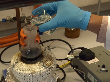
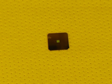
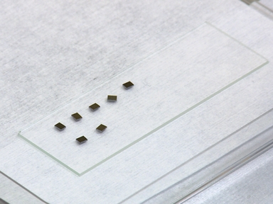
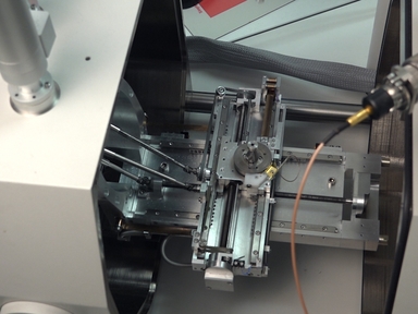
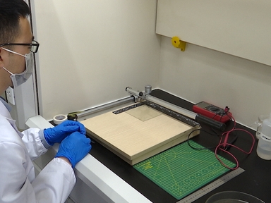
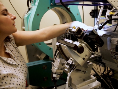
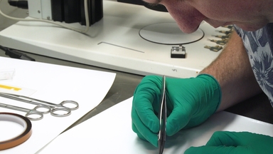
•A workflow for comprehensive micro-characterization of active optical devices is outlined. It contains structural as well as functional investigations by means of CT, LM and SEM. The method is demonstrated for a white LED which can be still be operated during characterization.
Tags
Related Videos
Energy Dispersive X-ray Tomography for 3D Elemental Mapping of Individual Nanoparticles

Failure Analysis of Batteries Using Synchrotron-based Hard X-ray Microtomography
Measurement of X-ray Beam Coherence along Multiple Directions Using 2-D Checkerboard Phase Grating

Dynamic Pore-scale Reservoir-condition Imaging of Reaction in Carbonates Using Synchrotron Fast Tomography
Studying Dynamic Processes of Nano-sized Objects in Liquid using Scanning Transmission Electron Microscopy
Precision Milling of Carbon Nanotube Forests Using Low Pressure Scanning Electron Microscopy
Enhanced Electron Injection and Exciton Confinement for Pure Blue Quantum-Dot Light-Emitting Diodes by Introducing Partially Oxidized Aluminum Cathode
Synchrotron X-ray Microdiffraction and Fluorescence Imaging of Mineral and Rock Samples
X-ray Beam Induced Current Measurements for Multi-Modal X-ray Microscopy of Solar Cells

Graphene-Assisted Quasi-van der Waals Epitaxy of AlN Film on Nano-Patterned Sapphire Substrate for Ultraviolet Light Emitting Diodes
Copyright © 2024 MyJoVE Corporation. 판권 소유