Aby wyświetlić tę treść, wymagana jest subskrypcja JoVE. Zaloguj się lub rozpocznij bezpłatny okres próbny.
Method Article
Utilization of Plasmonic and Photonic Crystal Nanostructures for Enhanced Micro- and Nanoparticle Manipulation
W tym Artykule
Podsumowanie
Plasmonic tweezers and photonic crystal nanostructures are shown to produce useful enhancements in the efficiency and orientation control of optically trapping micro- and nano-particles.
Streszczenie
A method to manipulate the position and orientation of submicron particles nondestructively would be an incredibly useful tool for basic biological research. Perhaps the most widely used physical force to achieve noninvasive manipulation of small particles has been dielectrophoresis(DEP).1 However, DEP on its own lacks the versatility and precision that are desired when manipulating cells since it is traditionally done with stationary electrodes. Optical tweezers, which utilize a three dimensional electromagnetic field gradient to exert forces on small particles, achieve this desired versatility and precision.2 However, a major drawback of this approach is the high radiation intensity required to achieve the necessary force to trap a particle which can damage biological samples.3 A solution that allows trapping and sorting with lower optical intensities are optoelectronic tweezers (OET) but OET's have limitations with fine manipulation of small particles; being DEP-based technology also puts constraint on the property of the solution.4,5
This video article will describe two methods that decrease the intensity of the radiation needed for optical manipulation of living cells and also describe a method for orientation control. The first method is plasmonic tweezers which use a random gold nanoparticle (AuNP) array as a substrate for the sample as shown in Figure 1. The AuNP array converts the incident photons into localized surface plasmons (LSP) which consist of resonant dipole moments that radiate and generate a patterned radiation field with a large gradient in the cell solution. Initial work on surface plasmon enhanced trapping by Righini et al and our own modeling have shown the fields generated by the plasmonic substrate reduce the initial intensity required by enhancing the gradient field that traps the particle.6,7,8 The plasmonic approach allows for fine orientation control of ellipsoidal particles and cells with low optical intensities because of more efficient optical energy conversion into mechanical energy and a dipole-dependent radiation field. These fields are shown in figure 2 and the low trapping intensities are detailed in figures 4 and 5. The main problems with plasmonic tweezers are that the LSP's generate a considerable amount of heat and the trapping is only two dimensional. This heat generates convective flows and thermophoresis which can be powerful enough to expel submicron particles from the trap.9,10 The second approach that we will describe is utilizing periodic dielectric nanostructures to scatter incident light very efficiently into diffraction modes, as shown in figure 6.11 Ideally, one would make this structure out of a dielectric material to avoid the same heating problems experienced with the plasmonic tweezers but in our approach an aluminum-coated diffraction grating is used as a one-dimensional periodic dielectric nanostructure. Although it is not a semiconductor, it did not experience significant heating and effectively trapped small particles with low trapping intensities, as shown in figure 7. Alignment of particles with the grating substrate conceptually validates the proposition that a 2-D photonic crystal could allow precise rotation of non-spherical micron sized particles.10 The efficiencies of these optical traps are increased due to the enhanced fields produced by the nanostructures described in this paper.
Protokół
1. Random Au Nanoparticle Array Fabrication 8,10,12,14
- The Au nanoparticle array is formed by first creating a template that is made of a dense layer of randomly adsorbed latex spheres with mean diameter of 454 nm. This is achieved by first evaporating gold on a glass coverslip to a thickness of 20 nm using chromium as the adhesion layer.
- The polystyrene sphere monolayer is then self-assembled by exposing the gold-coated substrate to a mixture of 1-ethyl-3-(3-dimethylaminopropyl) carbodiimide hydrochloride (EDC), latex sphere suspension and de-ionized water.
- The adsorption process is allowed to last for about one hour and the non-absorbed spheres are washed away with a copious amount of water.
- The formed monolayer is allowed to air dry.
- Finally, another 20 nm of gold is evaporated on the latex sphere monolayer to form the random gold nanoparticle array.
- If an SEM is available, the AuNP array can be seen under the SEM to look like Figure 1 and a diagram of the process is shown in figure 8.
2. Biological Sample Preparation9,11
- Sample preparation for optically trapping mouse cell nuclei is now shown.
- 3T3 Mouse cell nuclei tagged with Acridine Orange dye were obtained from the Tewari group at the Fred Hutchinson Cancer Research Center.
- 10% Bovine Serum Albumin (BSA) in phosphate buffered saline (PBS) is added to the mouse cell nuclei in a concentration of approximately 1 : 10 (BSA : Mouse Cell Nuclei). The BSA helps to prevent the nuclei from sticking to the substrate.
- Mix the solution using sonication.
- 5 uL of our solution is deposited onto the aluminum grating array coverslip. It is better to perform this step with the aluminum grating on the microscope stage so that you do not have to transport the sample after the solution is deposited.
- Two stacks of two 1"by 1" coverslips are used to support a fifth coverslip through which the sample is viewed.
- Position the sample under the microscope for viewing.
3. Method for Trapping
- The optical tweezers are constructed by sending a 35 mW helium neon laser through a Zeiss Axio Imager.D1M equipped with a GFP 17 filter set which is modified to allow for 633 nm laser radiation to reach the sample.
- A Zeiss LD EC Epiplan - NEOFLUAR 50x objective is used to image the cell nuclei which are approximately 5 micron in diameter.
- After the sample is placed under the objective, focus the microscope on the gold nanoparticle array or diffraction grating.
- Translate microscope vertically until focus is achieved on the nuclei which you desire to trap.
- Position laser trap spot over particle and the particle should then maintain its position in the laser spot even when the stage is translated.
4. Representative Results:
The random gold nanoparticle array procedures should deposit a monolayer of AuNP's that can be viewed under an SEM to look like Figure 1. The trapping force created by these plasmonic tweezers can be 10-20 times the force generated by standard optical tweezers. The minimum intensities required by the plasmonic tweezers to achieve particle confinement are shown for particles of various sizes in Figure 4.9,10 The diffraction grating achieved alignment and trapping with 20 times higher trapping efficiency than the gold nanodots and could achieve trapping with as little as 17 uW/um2 (Figure 7).11
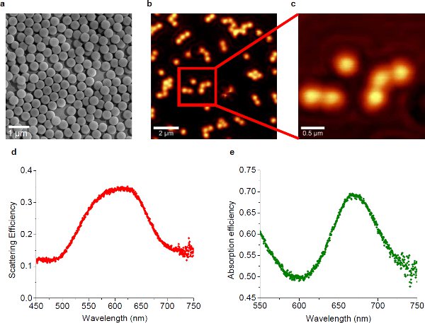
Figure 110 (a) SEM micrograph of the self-assembled gold nanoparticles. The diameter of individual gold nanoparticles is about 450 nm. (b) NSOM image of the plasmonic substrate where the nanoparticle distribution is sparse, showing the near-field radiation. The wavelength of the excitation laser is 633 nm. (c) High magnification view of the area marked with the red square in (b). (d) Scattering efficiency spectrum of the plasmonic substrate, showing the peak at 624 nm. (e) Absorption efficiency spectrum of the plasmonic substrate, showing the peak at 668 nm.
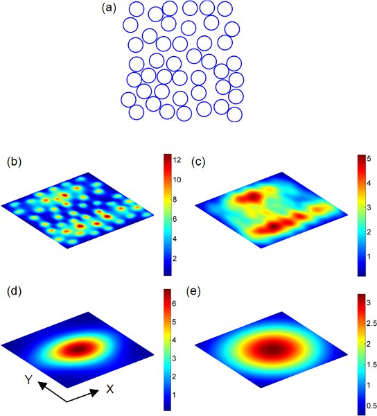
Figure 213 (a) Au nanospheres randomly distributed on a 2D domain 1 x 1 μm2. Each blue dot represent the center of the nanosphere (a = 60 nm). Scattering field distributions on observation planes which are parallel to the random nanosphere array are shown in (b) - (e). The nanosphere array is uniformly illuminated by a plane wave at the wavelength of 540 nm. The refractive index of the surrounding medium is 1.33. The polarization direction of the plane wave points along the X-axis (horizontal in (a)). The magnitude of the incident electric field is assumed to be 1 in the calculation. The separation between the observation plane and the nanosphere array is defined as h. b) h = a. c) h = 2a. d) h = λ. e) h = 2λ.
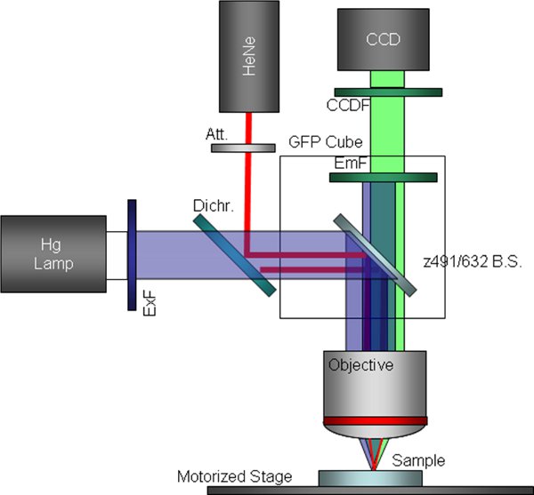
Figure 39 Schematic of customized fluorescence microscope configuration including a bypassed excitation filter and a replaced dichroic beam-splitter. This is the configuration used for simultaneous trapping and fluorescence imaging.
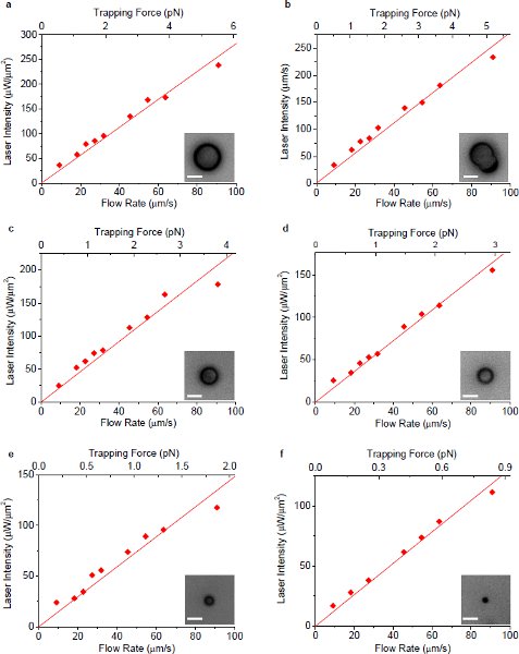
Figure 410 The minimum laser intensity to maintain the trap as a function of flow rate of surrounding fluid utilizing plasmonic trapping. All the optical intensities are measured at the sample plane under the microscope objective. (a) - (f) show the measurement results for single polystyrene beads with diameter 7.3, 6.3 (non-spherical), 5.0, 3.9, 2.5 and 1.1 μm, respectively. The insets show the corresponding microscopic images of particles. The scale bars in all images represent 5 μm in length.
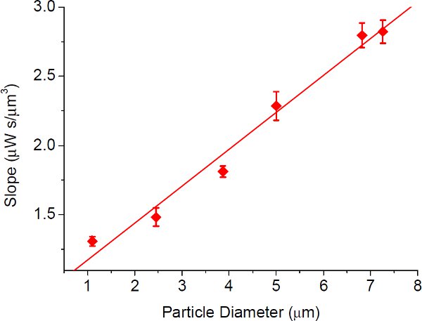
Figure 510 The slope of the fitted line through origin in Fig. 4 versus particle size for plasmonic trapping. The error bars show the standard deviations of the linear fits. The slope of the fitted line (ratio between the optical intensity threshold and flow rate) in Fig. 4 has an approximately linear relationship with particle size as shown in this figure, indicating the advantage of plasmonic trapping especially for smaller particles.
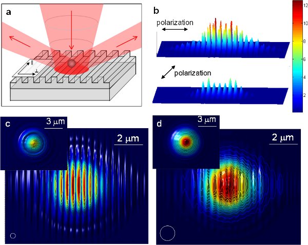
Figure 611 (a) Schematic drawing of the enhanced optical trapping utilizing 1-D periodic nanostructures. The incident beam is diffracted by the periodic nanostructure at far field. (b) The intensity distribution of light with two orthogonal polarizations nanostructure at far field. (b) The intensity distribution of light with two orthogonal polarizations at the surface of an aluminum grating with a 417 nm period obtained using FDTD simulations. The distribution is normalized to the intensity on a flat aluminum surface. (c) and (d) Trapping potential for particles directly above the grating surface versus location of the particle for (c) a 350 nm polystyrene bead and (d) a 1 μm polystyrene bead. The white circles illustrate the sizes of the particles. Insets show the trapping potential above a flat aluminum surface for the same particle size as comparisons. The values are normalized for each particle size. For all FDTD simulation figures the field of view is 10 x 8 μm2.
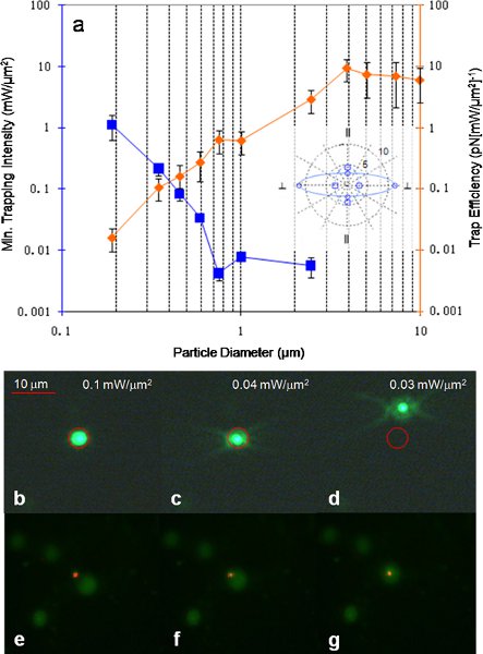
Figure 711 (a) Trap efficiency and minimum trapping intensity measured for polystyrene beads of various sizes with beam polarization perpendicular to grating lines. Inset shows trap asymmetry in trapping efficiency for translating a 3.87 um polystyrene bead perpendicular and parallel to the rules of the grating. The solid line (large asymmetry) is obtained with incident light polarized perpendicular to the grating, and the dash line (small asymmetry) is obtained with incident light polarized parallel to the grating. The unit is in (pN[mW/μm2]-1). (b)-(d) Trapping demonstration of a fluorescent 590 nm polystyrene bead. The red circle indicates the position of the laser spot as the laser light was too dim to be seen. At first the particle is trapped within the spot at higher power, as the power is lowered the Brownian motion of the particle overcomes the trapping force, allowing the particle to escape. (e)-(g) Trapping demonstration of a fluorescent ovarian cancer cell nucleus. The minimum intensity required to initiate trapping was 16 μW/μm2 obtained using a 20x objective lens.
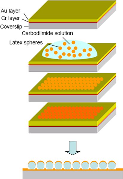
Figure 814 Fabrication procedure of the cap-shaped gold nanoparticles: a) Evaporation of the Cr and Au thin layer on the glass coverslip. b) Exposure to the polystyrene sphere suspension and adsorption of spheres for 1 hour. c) Removal of non-adsorbed polystyrene spheres and drying of the surface. d) Evaporation of another layer of Au on top of the template spheres. e) Schematic of the cap-shaped Au nanoparticle array, where Au only covers the top side of the template spheres.
Dyskusje
The significance of these methods of trapping is that they decrease the optical intensity necessary for sustained trapping from somewhere on the order of 103 μW/μm2 to somewhere on the order of 10 μW/μm2.10,11 The limitations on these techniques are that the gold nanoparticle array experiences heating issues that must be overcome. To overcome this issue, a 2D photonic crystal structure that is composed of a dielectric material can be used. Such a structure could the...
Ujawnienia
No conflicts of interest declared.
Podziękowania
We would also like to thank Xiaoyu Miao and Ben Wilson for developing the most of the methods described within. This work was funded by National Science Foundation (DBI 0454324) and the National Institute of Health (R21 EB005183) and by PHS NRSA T32 GM07270 from NIGMS to ECK.
Materiały
| Name | Company | Catalog Number | Comments |
| Material Name | Company | Catalog Number | Comment |
| Axio Imager Microscope (D1M) | Carl Zeiss, Inc. | D1M | Zeiss Axio Imager.D1M |
| Microscope Objective (50x/0.55) | Carl Zeiss, Inc. | LD EC Epiplan - NEOFLUAR 50x/0.55 HD DIC | |
| Zeiss Microscope Camera (AxioCam MRc) | Carl Zeiss, Inc. | ||
| Helium Neon Laser (35 mW) | Research Electro-Optics | ||
| Continuously Variable Attenuator | Thorlabs Inc. | NDC-100C-4M | For adjusting microscope intensity |
| Zeiss Filter Set #17 | Carl Zeiss, Inc. | 488017-9901-000 | Filter Set #17 |
| Microscope Slides, 0.5 mm thickness | VWR international | ||
| 3T3 mouse cell nuclei | Fred Hutchinson Cancer Research Center | Store as cold as possible | |
| Acridine Orange dye | Fred Hutchinson Cancer Research Center | ||
| Bovine Serum Albumin, 1 to 10 ration in PBS | Fred Hutchinson Cancer Research Center | ||
| 454 nm polystyrene latex spheres | Polysciences, Inc. | ||
| carbodiimide hydrochloride (EDC) - 1-ethyl-3-(3-dimethylaminopropyl) | G-Biosciences | BC25-1 | |
| gold (for deposition) | |||
| Reflective ruled diffraction grating | Edmund Scientific | ||
| Dulbecco’s Phosphate-Buffered Saline (D-PBS) (1X) | Invitrogen | 14190-144 |
Odniesienia
- Jones, T. B. . Electromechanics of Particles. , (1995).
- Ashkin, A. Optical trapping and manipulation of neutral particles using lasers. Proc. Natl. Acad. Sci. U.S.A. 94, 4853-4853 (1997).
- Neuman, K. C., Chadd, E. H., Liou, G. F., Bergman, K., Block, S. M. Characterization of photodamage to Escherichia coli in optical traps. Biophys. J. 77, 2856-2856 (1999).
- Chiou, P. C., Ohta, A. T., Wu, M. C. Massively parallel manipulation of single cells and microparticles using optical images. Nature. 436, 370-370 (2005).
- Hsu, H. Y., Ohta, A. T., Chiou, P. Y., Jamshidi, A., Nealea, S. L., Wua, M. C. Phototransistor-based optoelectronic tweezers for dynamic cell manipulation in cell culture media. Lab Chip. 10, 165-172 (2010).
- Righini, M., Ghenuche, P. S., Cherukulappurath, V., Myroshnychenko, F. J., Garcia de Abajo, R. Quidant Nano-optical Trapping of Rayleigh Particles Escherichia coli Bacteria with Resonant Optical Antennas. Nano Letters. 9, 3387-3391 (2009).
- Righini, M., Zelenina, A. S., Girard, C., Quidant, R. Parallel and Selective Trapping in a Patterned Plasmonic Landscape. Nature Physics. 3, 477-480 (2007).
- Miao, X., Lin, L. Y. Large dielectrophoresis force and torque induced by localized surface plasmon resonance of a cap-shaped Au nanoparticle array. Opt. Lett. 32, 295-297 (2007).
- Wilson, B. K. . Manipulation of Nanoparticles and Biological Samples through Enhanced Optical Forces [dissertation]. , (2009).
- Miao, X. Y., Wilson, B. K., Pun, S. H., Lin, L. Y. Optical manipulation of micron/submicron sized particles and biomolecules through plasmonics. Optics Exp. 16, 13517-13525 (2008).
- Wilson, B. K., Mentele, T., Bachar, S., Knouf, E., Bendoraite, A., Tewari, M., Pun, S. H., Lin, L. Y. Nanostructure-enhanced laser tweezers for efficient trapping and alignment of particles. Optics. Exp. 18, 16005-16013 (2010).
- Miao, X., Wilson, B. K., Cao, G., Pun, S. H., Lin, L. Y. Trapping and Rotation of Nanowires Assisted by Surface Plasmons. IEEE Journal of Selected Topics in Quantum Electronics. 15, 1515-1520 (2009).
- Miao, X. Y., Lin, L. Y. Trapping and manipulation of biological particles through a plasmonic platform. IEEE Journal of Selected Topics in Quantum Electronics. 13, 1655-1662 (2007).
- Miao, X. . Plasmonics for Micro/Nano Manipulation and Optofluidics [dissertation]. , (2008).
Przedruki i uprawnienia
Zapytaj o uprawnienia na użycie tekstu lub obrazów z tego artykułu JoVE
Zapytaj o uprawnieniaPrzeglądaj więcej artyków
This article has been published
Video Coming Soon
Copyright © 2025 MyJoVE Corporation. Wszelkie prawa zastrzeżone