Characterization of SiN Integrated Optical Phased Arrays on a Wafer-Scale Test Station
In This Article
Summary
Here, we describe the operation of a SiN integrated photonic circuit containing optical phased arrays. The circuits are used to emit low divergence laser beams in the near infrared and steer them in two dimensions.
Abstract
Optical phased arrays (OPAs) can produce low-divergence laser beams and can be used to control the emission angle electronically without the need for moving mechanical parts. This technology is particularly useful for beam steering applications. Here, we focus on OPAs integrated into SiN photonic circuits for a wavelength in the near infrared. A characterization method of such circuits is presented, which allows the output beam of integrated OPAs to be shaped and steered. Furthermore, using a wafer-scale characterization setup, several devices can easily be tested across multiple dies on a wafer. In this way, fabrication variations can be studied, and high-performance devices identified. Typical images of OPA beams are shown, including beams emitted from OPAs with and without a uniform waveguide length, and with varying numbers of channels. In addition, the evolution of output beams during the phase optimization process and beam steering in two dimensions is presented. Finally, a study of the variation in the beam divergence of identical devices is performed with respect to their position on the wafer.
Introduction
Optical phased arrays (OPAs) are advantageous due to their ability to shape and steer optical beams nonmechanically - this is useful in a broad range of technological applications such as light detection and ranging (LIDAR), free space communication and holographic displays1. The integration of OPAs in photonic circuits is of particular interest, as it provides a low cost solution for their fabrication with a small physical footprint. Integrated OPAs have been successfully demonstrated using a number of different material systems including InP, AlGaAs and silicon2,3,4. Of these systems, silicon photonics is perhaps the most convenient, due to its high refractive index contrast and compatibility with CMOS5. Indeed, OPA circuits have been extensively demonstrated in the silicon-on-insulator platform6,7,8,9,10; however, the application of these circuits is limited both by the wavelength transparency window of silicon and the high nonlinear losses, which lead to a limit on the available output optical power. We focus instead on OPAs integrated in SiN, a material with similar properties to silicon in terms of CMOS capability and footprint size11,12. In contrast to silicon however, SiN is expected to be suitable for a larger range of applications since the transparency window is broader, down to at least 500 nm, and thanks to the possibly high optical power thanks to the relatively low nonlinear losses.
The principals of OPA integration have recently been demonstrated using SiN8,13,14. Here, we will extend these principals to demonstrate a method of characterizing and operating integrated OPAs for two dimensional beam steering. In comparison to previous demonstrations of beam steering in two dimensions that rely on the tuning of the wavelength6, our circuit can operate at a single wavelength. We first provide a brief overview of the operating principles behind OPAs. This is followed by an introduction to the circuits used in this work. Finally, the characterization method is described and typical images of OPA output beams presented and discussed.
OPAs are composed of an array of closely spaced emitters that can be addressed individually to control the optical phase. If a linear phase relationship exists across the emitter array, the interference pattern in the far field yields several clearly separated maxima - similar to the principles of multi-slit interference. By controlling the magnitude of the phase difference, the position of the maxima can be adjusted, and hence, beam steering performed. In integrated OPAs, emitters consist of closely spaced diffraction gratings where the light is scattered and emitted out of the chip plane. A schematic illustration of an integrated OPA device is shown in Figure 1A,B. Light is coupled into the chip, in this case via an optical fiber, and is then divided into multiple channels, each containing an integrated phase shifter. At the other end of the optical circuit, the waveguides terminate in gratings and combine to form the OPA. The resulting output beam is comprised of multiple interference maxima, the brightest of which is referred to as the fundamental lobe and is the one most often used in beam steering applications. The emission direction of the fundamental lobe is defined by the two azimuthal angles to the orthogonal projection of the chip plane, φ and θ, perpendicular and parallel to the orientation of the grating respectively. In this document, φ and θ will be referred to as the 'perpendicular' and 'parallel' emission angles, respectively. The perpendicular angle φ is determined by the phase difference between the OPA channels, and the parallel angle θ depends on the period of the output gratings.
Our integrated circuits are fabricated using Si3N4 waveguides with a cross section of 600 x 300 nm2, a design that was optimized for the fundamental transverse electric polarization mode of light at a wavelength of 905 nm. Underneath the waveguides lies a 2.5 µm SiO2 buffer layer on top of a silicon wafer. The thermal phase shifters were made from a 10(100) nm thick Ti(TiN) layer used to form 500 µm long and 2 µm wide resistive wires. In our circuits, an electric power of 90 mW is required to achieve a phase shift of π. The OPA output gratings consist of 750 fully etched periods with a nominal filling factor of 0.5 and a grating period between 670 nm and 700 nm. Further information on the platform design and fabrication is given in Tyler et al.15,16.
In this work, two different types of circuits are characterized, a passive circuit without phase shifting capabilities, and a more complex circuit, designed to perform beam steering in two dimensions. The two dimensional beam steering circuit is shown in Figure 2. Figure 2A contains a schematic of the circuit and Figure 2B shows a microscope image of the fabricated device. The light enters the circuit at the input grating. It then reaches a switching network where it can be routed selectively towards one of four sub-circuits. Each sub-circuit splits the light into four channels using multimode interference devices (MMI). The channels each contain a thermal phase shifter and form an OPA at the end of the circuit. The four OPAs originating from the four sub-circuits each comprise a different grating period between 670 nm and 700 nm. These periods correspond to azimuthal angles parallel to the grating axis, θ, between 7° and 10°. A more detailed description on the circuit can be found in Tyler et al.16.
The presented characterization setup is based on an automated probing station capable of performing a series of measurements on many circuits across a whole wafer. This enables study of the performance variation relative to the position on the wafer and to select the devices with the optimum properties. However, the use of a prober station implies some physical constraints to the OPA characterization scheme due to the relatively small available space above the wafer. The characterization of optical phased arrays requires imaging the OPA output in the far field, which can be performed in a number of ways. For example, a series of lenses may be used in a Fourier imaging system6 or the farfield image formed on a Lambertian surface may be viewed in either reflection or transmission. For our system, we chose what we considered to be the simplest and most compact solution of placing a large surface 35 mm x 28 mm CMOS sensor without lenses placed approximately 50 mm above the wafer surface. Despite the increased cost of such a large CCD sensor, this solution allows a sufficient field of view without the use of lenses.
Protocol
1. Preparations
- Prepare the following experimental setup (Figure 4).
- Use a computer.
- Use a continuous wave fiber coupled laser source. Depending on the circuit losses, 1 mW power suffices. In the presented characterization setup, the laser source is at a wavelength of 905 nm.
- Use a polarization controller adapted for the laser wavelength.
- Use a cleaved input fiber to couple light into the input grating coupler of the optical circuit.
- Use an electric probe to connect the electronic control board to the electrical contact of the optical circuit.
- Use a system capable of controlling the 20 phase modulators of the two dimensional beam steering circuit is required. In the presented characterization setup, this system is a custom electronic board controlled by an Arduino, which is able to apply individually between 0 and 200 mW of electric power at the phase shifters on the optical circuit. A schematic of the electrical circuit is shown in Figure 3. For each channel, the circuit contain a DAC (Digital to Analog Converter) that will translate the digital command voltage to an analog voltage that controls the gate of a high-power transistor. The heater is connected to a high-power current source. Therefore, by controlling the gate tension, the current flow in the heater can be adjusted.
- Use a bare image sensor to image the far field of the optical output. In the presented characterization setup, the camera is a 35 mm CCD sensor.
- Use a optical microscope in order to image the chip for alignment purposes.
- Use a 3-axis translation stage and mount to fit a 200 mm wafer. In the presented characterization setup, this stage is a reconfigurable probe system for silicon photonics.
- Equipment assembly
- Assemble the equipment according to Figure 4 and mount the wafer. The distance between wafer and the sensor needs to be chosen small enough to ensure a high-resolution image of the output beam, but large enough to fit at least two interference maxima in order to be able to find the relationship between sensor pixels and output angle as will be explained in section 4 of the protocol.
- Ensure that the sensor and the wafer are parallel; otherwise, it may falsify the computation of the pixel/output angle computation. In the presented characterization setup, set the wafer-sensor distance to 5 cm. If a double sensor configuration is used (like the one presented here), ensure that the bare sensor can easily be removed to give access to the optical microscope in order to image the near-field for fiber alignment purposes.
- Be sure that the electrical probe, camera and optical fiber are not touching each other. Connect required elements to a computer. In the presented setup the probe station, the CCD sensor and the electrical circuit for the phase control are driven via a computer and a Python program in order to automate the measurement process.
2. Optical coupling
- Fiber alignment
- Using the microscope, start by carefully lowering the fiber until it touches the wafer surface (away from the input grating coupler to avoid damaging it), and then move it up about 20 µm.
- When this is done, maximize the light intensity at the output gratings. To do so, start sweeping the fiber position over the OPA input grating coupler. If the camera attached to the microscope is responsive to the laser wavelength (if not use the bare image sensor), and if the fiber and grating coupler are well aligned, light exiting at the OPA output gratings should be visible on the image. An example can be seen in Figure 5A.
- When light is seen from the OPA antennas, adjust the polarization in order to maximize the light intensity at the output gratings. Be sure to avoid any movement or vibration of the input fiber
- OPA output imaging
- Switch to the far-field imaging sensor and improve the image quality: Adjust both the exposure time of the sensor and the laser power in such a way that the OPA output is clearly visible on the camera and the beam does not saturate the sensor. An example image recorded by the sensor is shown in Figure 5B.
- If necessary, cover the setup so that the background light does not interfere with the image from the OPA beam. Generally, the weaker the background light, the lower the laser power that can be set.
- Block the reflections by placing a highly reflecting sheet between the reflection and the camera. Sometimes, reflections originating from the wafer surface reach the sensor area and contaminate the image of the OPA output (reflections can happen at the input grating).
- Readjust the polarization of the input light to obtain a clear image.
3. Beam optimization and steering
NOTE: This section describes the operation of the circuit shown in Figure 2 and how it can be used to perform beam steering in two dimensions.
- Preparations
- Connect the electric circuit for the phase control to a multi-channel electric probe.
- Using the microscope, connect the pins of the electric probe to the metal contact pads of the optical circuit.
- Re-optimize the position of the input fiber.
- Switch to the far field sensor and image the output.
- Selection of the parallel emission angle θ using the switching network
- Study the ring resonators of the switching network in order to control the emission angle in θ. For this purpose, observe the far field image of the output while varying the voltages applied to the phase shifters at the ring resonators. With the correct voltage applied to each resonator, a different area on the sensor will be illuminated, corresponding to a certain θ value, as shown in Figure 6B.
- Find the voltages where the rings are on- and off-resonance. For this purpose, an automated script can be used to sweep the resonator voltages and record the intensities on the different θ areas on the sensor. Use found voltages to access the various sub-circuits and to steer the output beam in θ.
- Selection of the orthogonal emission angle φ by optimizing the OPA phases
- Optimize the OPA phases in order to shape and steer the output beam in φ. For this purpose, select a small pixel area (corresponding to the desired φ angle) that should be illuminated with a focused output beam.
- Maximize the brightness inside the chosen area by running the following the optimization routine.
- Shift the phase of one of the OPA channels in small increments. After each shift, record the integral of the brightness in the pixel area inside, Ii, and outside, Io, of the selected area. Calculate the ratio R = Ii / Io. After a full phase shift cycle between 0 and 2π, apply the phase shift with the highest recorded brightness ratio R.
- Repeat this phase optimization process on the next OPA channel. Different optimization algorithms may be used, such as a hill climbing.
- Repeat the optimization process by optimizing the phases until the optimization process is saturated and a focused output beam is visible. Example images of the output beam taken during an optimization process is shown in Figure 6A. After 16 optimization rounds, the output beam a focused beam is visible.
NOTE: If some additional unexpected peaks are present, this may be a result of a temporally unstable coupling into the circuit during the optimization process. This may be due to movement of the input fiber and/or an unstable polarization state.
- In order to steer the output beam to a different φ angle, select a new pixel area and repeat the optimization process.
4. Beam divergence measurements and image analysis
- Image acquisition
- Optimize the position of the input fiber. Record the image of the output in the far-field. Make sure that at least two clear interference maxima are visible.
- Using the alignment system, move the wafer in order to align the next device to the input fiber. Perform fine alignment by maximizing the output intensity recorded by the camera. Record output image.
- Repeat the above step until all devices of interest have been characterized. If the selected optical circuit has the capability of phase adjustment of the OPA channels, perform a phase optimization routine before recording the images.
- Image analysis
- Check the recorded images for false data points arising from defective pixels, such as dead or hot pixels. Erase these data points or replace the values by typical values.
- Correlate the CCD pixels to OPA output angles φ and θ as follows.
- Calculate the angular distance Δφ between the interference maxima according to the OPA design using Δφ = sin-1(λ/d) [°], where λ is the wavelength and d is the lateral pitch between the OPA gratings. Fit two Gaussian curves to the two interference maxima and determine the positions of the two centers, P1 and P2. Since the distance (in pixels) between the two centers, N = P2 - P1, is expected to correspond to Δφ, we obtain a conversion factor c between pixel and angle c = Δφ/N [°/pixel], which can be used to obtain a relative angle relationship between pixels.
- Obtain the conversion factor, c, via an accurate measurement of the distance between the wafer surface and the sensor, and the pixel size (5.5*5.5µm for the sensor used here).
- Estimate the absolute output angles in φ and θ for one of the CCD pixels. Set the beam center in θ to the expected emission angle according to simulations. In order to choose the absolute value in φ, optimize the beam for several angles in φ by adjusting the OPA phases, and record the intensity of the main lobe for each angle. According to the OPA theory, the main lobe is most intense (and the intensity in the side lobes minimized) when emitting at φ = 0°. Hence, set the pixel in the center of the beam with the maximum recorded beam intensity, to φ = 0°. Use this pixel and the conversion factor to assign absolute angles to all pixels of the image.
- In the case of an output beam with significant tilt with respect to the vertical axis, and if the beam divergence and position must be measured very accurately, tilt the camera in order to be perfectly perpendicular to the output beam. Otherwise, it is also possible to apply a correction factor to the measured beam size by computing the projection of the beam on the sensor depending on the angle between the output beam and camera plane.
- Calculation of the beam divergence
- Extract cross sections across the center of the fundamental beam along φ and θ.
- Fit two Gaussian curves to the cross sections and extract the full-width-at-half-maxima as a measure for the beam divergence φdiv and θdiv.
- Calculate the expected beam width φdiv = λ/Nd [°], where λ is the wavelength and d the lateral distance between the OPA gratings.
- Estimate the beam divergence θdiv by performing FDTD simulations of the output gratings.
- Automatic testing
- If the characterization bench (as the one presented here) can perform automated measurements, perform some additional steps. First, obtain the chip dimensions and the coordinates of the measured structures from the circuit layout. Then, input those values to the bench control software. Therefore, once the input fiber have been aligned on the first tested structure (as detailed in section 2.1), the bench can switch automatically from one structure to another via a translation of the wafer.
Representative Results
In this section, several in operando images of OPA beams are shown. These include images in the near and the far field of the beam, OPA output beams before and after phase optimization, and beams with a varying number of OPA channels.
An image of the near field of the beam, recorded using the microscope, can be seen in Figure 5A. The picture shows a passive OPA circuit with a large number of channels and the light emitted at the OPA gratings is clearly visible. This circuit produces an interference pattern in the far-field, which was recorded using the CCD sensor. The sensor image is given in Figure 5B and shows both the fundamental lobe as well as a side lobe. The exposure time of the sensor, the laser power and the background light have been optimized to produce a clear image. The two maxima are separated by 17.6°, calculated according to the equation given in the protocol section 4.2.2.1. Note that in this design, all waveguides are of the same length and therefore no significant phase difference between the channels is present. As a result, the interference maxima are clearly separated. An example of an OPA circuit with an irregular phase difference between the channels is presented below.
In order to observe clear interference maxima in the OPA output pattern, a linear phase difference between the OPA channels is required. However, when the length of the waveguides between the input and the output gratings varies from channel to channel, the interference pattern will show multiple, irregular interference sections along a straight line in the direction perpendicular to the grating orientation (i.e., along angle φ). An example of such an output pattern is given in the top left image of Figure 6A. It shows the far-field output of a 16-channel OPA with a non-uniform waveguide length between the input and output gratings. Fortunately, this OPA design has phase shifters included in every channel, so that the phases can be adjusted individually and the output beam shaped. After optimizing the phases as described in protocol section 3.3, the output beam forms one clear maximum. Figure 6A shows how the output beam evolves during the optimization process. Note that further interference maxima are present outside of the sensor area. In addition, we observe that the beam divergence of the 16-channels OPA is much broader than that seen in Figure 5B. This effect is expected and is due to a significant reduction in the channel number.
In the following, the operation of the optical circuit for OPA steering in two dimensions will be discussed, for details on the circuit see Figure 2. Firstly, the ring voltages of the switching network were calibrated in order to route the light to the different sub-circuits, each containing an OPA. Since the four OPAs each comprise a different grating period, routing the light between the sub-circuit results in the output beam being emitted at different θ angles. This is shown in Figure 6B, which contains the far-field images recorded as the light path is altered using the ring resonators of the switching network. The images show that the 'parallel' emission angle, θ, changes as each individual resonator is set on-resonance with the input light, while tuning the other resonators off-resonance. Our circuit was designed to access four different θ angles, however, due to a design error in the switching network, it was only possible to operate three of the ring resonators. From the output images, we can see that the interference pattern is irregular and no clear maxima are visible. In order to steer and shape the output beam in the 'perpendicular' emission angle, φ, the OPA phases were adjusted and optimized.
An example image of an optimized output beam of the two dimensional beam steering circuit is shown in Figure 7A. Two interference maxima are clearly visible, corresponding to the main lobe and one of the side lobes. The top image in Figure 7A shows a heat map of the recorded brightness at the sensor versus pixel number. In order to determine the output angle, the image was processed as described in section 4.2 of the protocol and the relationship between pixel number and output angle determined. The calibrated image of beam intensity versus angle is shown in the bottom-most image of Figure 7A.
In the following, the beam steering results will be discussed. The OPA beam was successfully steered in an area of 17.6° × 3° (φ × θ), example data is shown in Figure 7B and Figure 7C. Figure 7B shows images of the beam being steered in φ while maintaining θ constant at 8°. This was achieved by first accessing the OPA corresponding to a parallel emission angle of θ = 8° and subsequently varying the optical phases to change the perpendicular emission angle, φ. Normalized intensity plots of the fundamental beam steered to three different output positions in θ are shown in Figure 7C, with a fixed perpendicular emission angle of φ = -2.5° and θ varying between 7° and 9°. As before, the parallel emission angle θ was controlled using the ring resonator network to switch between the OPAs. After OPA selection, the OPA phases were optimized to emit at φ = -2.5°.
Finally, the beam divergence was determined by fitting two Gaussian curves along φ and θ as described in protocol section 4.3. The FWHM serves as a measure for the beam divergence and was measured to be 4.3° in φ and 0.7° in θ for emission angles of φ = -2.5° and θ = 8°, see Figure 8A. These values are in good agreement with the expected values of 4.3° and 0.6° in φ and θ, respectively, for a four-channel OPA, as described in sections 4.3.3 and 4.3.4 of the protocol. In addition to determining the divergence of a four channel OPA, we investigated the divergence of an OPA design with a much larger number of channels. The divergence of a passive OPA consisting of 128 channels, with a design similar to that shown in Figure 5A, was measured. In order to test for fabrication variations across a wafer, we launched an automatic scan to characterize 42 devices with identical designs. The recorded images were analyzed with respect to the beam divergence. The divergence in φ versus position of the device on the wafer is shown in Figure 8B. The measured values lie between 0.19° and 0.37° and are slightly larger than the expected value of 0.14°. This could be explained by phase errors inside the individual OPA channels. All waveguides in the design are of the same length and therefore theoretically no phase differences should arise between the OPA channels. However, fabrication errors result in uncontrolled phase shifts as the light travels from the input to the output gratings, which leads to a broadening of the output beam. Due to the absence of phase shifters in the circuit, it was not possible to compensate for these errors. As mentioned, the θ angle is defined by the antenna grating geometry. Therefore, fabrication variations (SiN film height and structures lateral dimensions deviation) could affect the OPA output angle, θ. Such variations have been characterized on 40 devices across the whole wafer. Thanks to the very well controlled CMOS fabrication process, a negligible 3σ (three times the standard deviation) of 0.156° has been found.
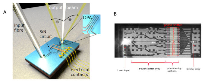
Figure 1: Illustration of integrated OPA. (A) The first-order interference lobe of the OPA output leaves the circuit at two azimuthal angles to the orthogonal projection of the chip plane, φ and θ, perpendicular and parallel to the orientation of the grating respectively. (B) Top view of an OPA showing its main constitutive elements. Please click here to view a larger version of this figure.
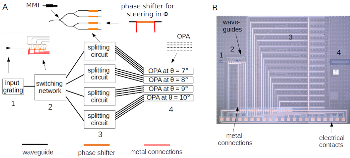
Figure 2: Schematic and microscope image of the integrated optical circuit for two dimensional beam steering. (A) Circuit containing a switching network connected to four sub-circuits, each forming an OPA. The output area contains four OPAs with four different grating periods and hence emission angles in θ. (B) Microscope image of the circuit described in (A), fabricated using SiN waveguides and Ti/TiN thermal phase shifters. Please click here to view a larger version of this figure.
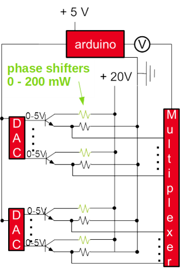
Figure 3: Electric circuit to apply electrical powers between 0 mW and 200 mW. This schematic represents an electric circuit which can individually apply voltages to the phase shifters in the optical circuit and read out their electrical current after voltage application. In our optical circuits, the phase shifters consist of electric wires with resistances of 1.3 kΩ. An electric power of 90 mW is required to achieve an optical phase shift of π. The circuit is controlled via an Arduino microcontroller. Please click here to view a larger version of this figure.
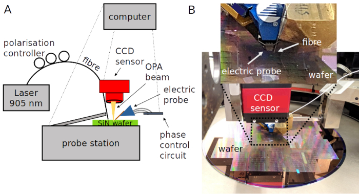
Figure 4: Experimental set-up for OPA circuit characterization. (A) Schematic of the experimental set-up. (B) Picture of the experiment. Please click here to view a larger version of this figure.
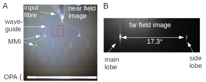
Figure 5: Near- and far field images of the output beam. (A) Near field image of an OPA circuit. Light at a wavelength of 905 nm is coupled into the circuit via a fiber and an input grating. Scattering of light inside the waveguides allows us to see the circuit design. At the end of an MMI tree, the light is emitted at the OPA gratings. (B) Far field image of the output of the circuit shown in (A). Two interference maxima are visible on the sensor. According to the OPA theory, the maxima are separated by 17.6°. Please click here to view a larger version of this figure.

Figure 6: OPA beam optimization and switching network operation. (A) OPA beam optimization of a 16-channel OPA using phase shifters. Far-field images are shown after each optimization step. After optimising all 16 channels, the beam forms one main interference maximum inside the sensor area. (B) By using a switching network consisting of ring resonators, different OPAs each comprising a different grating period is accessed. The different grating periods result in the output beam emitting at different θ angles. Please click here to view a larger version of this figure.
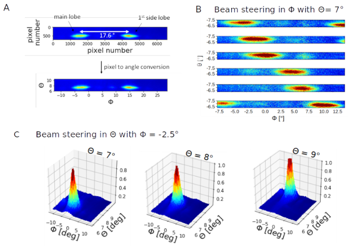
Figure 7: Characterization of the two dimensional beam steering circuit. (A) Pixel to angle conversion of the recorded image data. Beam steering results in φ and in θ are shown in (B) and (C), respectively. This figure has been modified from Tyler et al.16. Please click here to view a larger version of this figure.
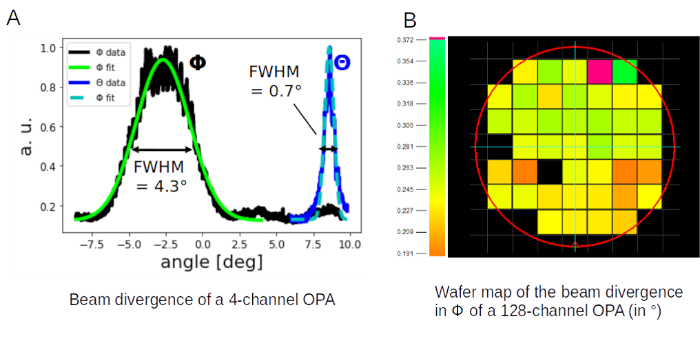
Figure 8: OPA beam divergence measurements. (A) Beam divergence analysis of a 4-channel OPA. This figure has been modified from Tyler et al.16. (B) Wafer map of measured divergences in φ of a 128 channel OPA design. Please click here to view a larger version of this figure.
Discussion
We have presented a method to characterize an integrated OPA. The main advantage of the method is the ability to easily probe multiple dies across a wafer, to look for fabrication variations and to identify high-performance devices. This can be seen in Figure 8B. From the wafer scan, it becomes clear that the lower half of the wafer exhibits devices with lower beam divergences. This could be explained by a higher waveguide quality in that area, which reduces random phase shifts and hence the beam divergence.
Using a large area CCD sensor to image the far field output is a convenient method to image the free space output of integrated circuits, since it can easily be added to most characterization set-ups due to their compact size in comparison to the often used, bulkier, Fourier-imaging systems6.
In order to guarantee a high accuracy of the beam angle and divergence measurement, particular care must be taken during the camera - OPA alignment. Moreover, the OPA response is sensitive to phase and polarization instabilities during calibration. Therefore, all sources of perturbation must be controlled: movement/vibration of the injection fiber, laser temperature, incoming light polarization etc.
In summary, a method to characterize integrated OPAs was presented. Details on how to couple light, how to control phase shifters in the circuit and how to image the output in the near and the far field were given. Typical images of the output beams of several OPA circuits were shown, including the results of beam steering in two dimensions at a single wavelength in the near infrared. Furthermore, we show the results of measuring multiple devices with the same design across a wafer in terms of beam divergence. A performance trend with respect to the position on the wafer was found, identifying areas with high-quality fabrication properties.
Acknowledgements
This work was funded by the French Direction Générale des Entreprises (DGE) via the DEMO3S project.
Materials
| Name | Company | Catalog Number | Comments |
| 25 ch electrical Probe | Cascade Microtech | InfinityQuad 25ch | |
| 35 mm CCD sensor | Allied Vision | Prosilica GT 6600 | |
| Arduino uno | Arduino | A100066 | |
| laser | Qphotonics | QFLD-905-10S | |
| optical fibre | Corning | HI780 | |
| polarization controller | ThorLabs | FPC023 | |
| prober station | Cascade Microtech | Elite 300 |
References
- Heck, M. J. Highly integrated optical phased arrays: Photonic integrated circuits for optical beam shaping and beam steering. Nanophotonics. 6 (1), 93-107 (2017).
- Vasey, F., Reinhart, F. K., Houdré, R., Stauffer, J. M. Spatial optical beam steering with an AlGaAs integrated phased array. Applied Optics. 32 (18), 3220-3232 (1993).
- Van Acoleyen, K., et al. Off-chip beam steering with a one-dimensional optical phased array on silicon-on-insulator. Optics Letters. 34 (9), 1477-1479 (2009).
- Guo, W., et al. Two dimensional optical beam steering with InP-based photonic integrated circuits. IEEE Journal of Selected Topics in Quantum Electronics. 19 (4), 6100212 (2013).
- Jalali, B., Fathpour, S. Silicon photonics. Journal of Lightwave Technology. 24 (12), 4600-4615 (2006).
- Hulme, J. C. Fully integrated hybrid silicon two dimensional beam scanner. Optics Express. 23 (5), 5861-5874 (2015).
- Chung, S., Abediasl, H., Hashemi, H. A monolithically integrated large-scale optical phased array in silicon-on-insulator CMOS. IEEE Journal of Solid-State Circuits. 53 (1), 275-296 (2018).
- Poulton, C. V., et al. Large-scale silicon nitride nanophotonic phased arrays at infrared and visible wavelengths. Optics Letters. 42 (1), 21-24 (2017).
- Poulton, C. V., et al. Coherent solid-state LIDAR with silicon photonic optical phased arrays. Optics Letters. 42 (20), 4091-4094 (2017).
- Martin, A., et al. Photonic integrated circuit based FMCW coherent LiDAR. Journal of Lightwave Technology. 36 (19), 4640-4645 (2018).
- Subramanian, A. Z., et al. Low-Loss Single mode PECVD Silicon Nitride Photonic Wire Waveguides for 532-900 nm Wavelength Window Fabricated Within a CMOS Pilot Line. IEEE Photonics Journal. 5 (6), 2202809 (2013).
- Baets, R., et al. Silicon Photonics: silicon nitride versus silicon-on-insulator. Optical Fiber Communication Conference, OSA Technical Digest (online) (Optical Society of America). , (2016).
- Sabouri, S., Jamshidi, K. Design Considerations of Silicon Nitride Optical Phased Array for Visible Light Communications. IEEE Journal of Selected Topics in Quantum Electronics. 24 (6), (2018).
- Zadka, M., et al. On-chip platform for a phased array with minimal beam divergence and wide field-of-view. Optics Express. 26 (3), 2528-2534 (2018).
- Tyler, N. A., et al. SiN Integrated Photonics for near-infrared LIDAR. 2018 IEEE CPMT Symposium Japan (ICSJ). , 63-66 (2018).
- Tyler, N. A., et al. SiN integrated optical phased arrays for 2-dimensional beam steering at a single near-infrared wavelength. Optics Express. 27 (4), 5851-5858 (2019).
This article has been published
Video Coming Soon
ABOUT JoVE
Copyright © 2024 MyJoVE Corporation. All rights reserved