Studying the Effects of Temperature on the Nucleation and Growth of Nanoparticles by Liquid-Cell Transmission Electron Microscopy
In This Article
Summary
Temperature control during liquid-phase electron microscopy experiments opens up new perspectives of studying the dynamic of nanoparticles in liquid environments mimicking their formation or application media. Using recently developed heating liquid cells, we directly observed the influence of temperature on the nucleation and growth processes of gold nanoparticles in water.
Abstract
Temperature control is a recent development that provides an additional degree of freedom to study nanochemistry by liquid cell transmission electron microscopy. In this paper, we describe how to prepare an in situ heating experiment for studying the effect of temperature on the formation of gold nanoparticles driven by radiolysis in water. The protocol of the experiment is fairly simple involving a special liquid cell with uniform heating capabilities up to 100 °C, a liquid-cell TEM holder with flow capabilities and an integrated interface for controlling the temperature. We show that the nucleation and growth mechanisms of gold nanoparticles are drastically impacted by the temperature in liquid cell. Using STEM imaging and nanodiffraction, the evolution of the density, size, shape and atomic structure of the growing nanoparticles are revealed in real time. Automated image processing algorithms are exploited to extract useful quantitative data from video sequences, such as the nucleation and growth rates of nanoparticles. This approach provides new inputs for understanding the complex physico-chemical processes at play during the liquid-phase synthesis of nanomaterials.
Introduction
Metal nanoparticles (NPs) have promising physico-chemical properties that can be used in various domains such as optical sensing1, medicine2 or energy3. Wet-chemical synthesis is a very versatile method to fabricate metal NPs with well-defined size and shape. Over the last decades, many strategies have been developed to gain control over NPs synthesis: seed-mediated growth4, face-blocking method5, kinetically-controlled synthesis6, selective etching7 or temperature-controlled synthesis8. However, while the chemical reactions driving the synthesis are fairly simple, the nucleation and growth mechanisms are not, because many parameters play a role in the formation processes and their individual influence are difficult to retrieve from ex situ snapshots of the resulting nanomaterials extracted from their formation medium at given time points of the synthesis. To truly understand the nucleation and growth processes and establish ways to control them, we must employ in situ tools that allow their real time observation in finely controlled liquid environment.
In that regards, Liquid-Cell Transmission Electron Microscopy (LCTEM) has been a very powerful method for shedding new light on the synthesis of metallic nanoparticles9,10,11,12,13. By imaging the dynamics of individual nanostructures directly in their liquid formation media, this technique has provided a deeper understanding of nucleation and growth mechanisms, notably the role of crystal defects, seed morphology and organic ligands that allow driving directional growth or etching processes and obtaining nanomaterials with specific shapes (nanorods, nanostars, nanoplates, nanoshells)10,11,12,13,14,15,16,17,18,19. When the electron beam of a TEM interacts with liquids, radiolysis processes produce strong reducing and oxidizing species that modifies the solution chemistry in the irradiated area and can be used to drive growth or etching processes. Interestingly, the concentration of radiolytic products is known to increase with the electron dose rate, a parameter that can be finely tuned in an electron microscope20. Therefore, this dose-rate dependency of radiolysis has been exploited to control the reaction speed and reveal kinetic effects on the formation processes and final morphology of nanostructures11,15,20.
Although the temperature is a crucial parameter in nanomaterials synthesis, its effects have so far not been carefully investigated by LCTEM, because commercial liquid-cells with reliable temperature control have only recently been developed. Yet, such in situ studies are indispensable to unravel the complex kinetics and thermodynamic effects induce by temperature changes. Indeed, on the one hand increasing the temperature has drastic impacts on the faceting processes during the growth, speeds up atomic and molecular diffusion in liquid and modifies the reaction rates. On the other hand, the nano-phase diagram of nanostructures is also very sensitive to temperature. In this article, we exploit recently developed heating liquid cells to follow the radiolytic growth of gold nanoparticles in water with a temperature control between room temperature and 100 °C. This methodology combining STEM imaging and diffraction in an environment that is getting closer and closer to the real synthesis conditions reduces the gap between in situ TEM observations and bench-scale syntheses.
Protocol
1. Align the transmission electron microscope for STEM HAADF imaging
- Follow manufacturer instructions for microscope alignment.
- Use a conventional dried sample to align the microscope. Do not use a liquid sample.
- To minimize the growth speed, minimize the electron dose rate (see discussion section) which implies using small condenser aperture and small spot size to reduce the beam current.
2. E-chip handling
NOTE: Commercial liquid-holders fit on almost all TEM but use the holder that is specifically design for the microscope brand and pole piece. A liquid cell is made of two MEMS-based silicon chips called E-chips, both of which are silicon substrates with a 500 x 50 µm window covered by a 50 nm thick amorphous silicon nitride (SiN) film that is electron transparent (Figure 1A). These two e-chips have different sizes. The small one is 2 x 2 mm with gold spacers that fix the distance between the two E-chips (150 nm here) and the liquid thickness. The large one is 4 x 6 mm and it has a resistance embedded inside the silicon substrate that allows a uniform heating of the liquid sample (Figure 1B). Because of the way they are fabricated in clean rooms, the E-chips have two different sides: one where the window looks small (here after called the front side) and the other where the window is large with a sink shape (here after called the back side).
- When handling the E-chips, never touch the window with tweezers and grip the chips by the sides. To avoid scratching the surface of the silicon substrate use carbon-tipped tweezers.
- If placing an E-chip on a surface, make sure that the back side is in contact with the surface because the SiN film is fragile and it is deposited on the front side.
3. Cleaning of the liquid cell holder (before the experiment)
- Remove the lid covering the tip of the holder. Remove the dummy liquid cells using tweezers. Remove the gasket used with the dummy liquid cells.
NOTE: Dummy liquid cells are liquid cells without the SiN window and only silicon. They are used for storing the liquid cell holder in the vacuum pump. Pay attention to the state of brass screws because they crumble easily over time. Particularly, if the screw heads are damaged, the screws must be changed. Otherwise, it may be difficult to unscrew them after the experiment and small debris may also disrupt sample loading. - Manually inject 2 mL of distilled water inside the holder using syringes and the external PEEK tubing to connect to the back of the holder.
NOTE: There are 3 microfluidic tunnels inside the holder. All three must be cleaned up with water. Pay attention to the water coming out of front of the holder: if the water is colored because of a previous experiment, continue to put water inside the holder until the liquid is uncolored. - If injecting a solution in the liquid cell during the experiment (1 mM of HAuCl4 in water in our case), fill the tubing of the sample holder with this solution.
- Dry up the tip of the liquid-cell holder using an air pistol.
4. Preparation of the liquid cell (E-chips)
- Cleaning of the liquid cells.
- Fill a glass Petri dish with acetone.
- Fill a glass Petri dish with methanol.
CAUTION: Due to the toxicity of methanol, the Petri dish with methanol must be put under a fume hood. Methanol should be handled with the adequate protective gear (gloves). - Put one small and one large E-chip in the Petri dish with acetone and wait for 2 minutes.
NOTE: The E-chips are coated with a protective layer that needs to be removed before the experiment. Acetone will remove the photoresist and clean up the E-chips of debris. To enhance the cleaning, the solution can be gently agitated. - Put both E-chips in the Petri dish with methanol and wait for 2 minutes. The methanol will clean up the E-chips from the acetone and the rest of the debris.
CAUTION: The transfer of the E-chips between the acetone and the methanol must be done as fast as possible in order to not let the E-chips dry up in the air. - Dry up the liquid cells using an air pistol. Hold the E-chip using tweezers while using the air pistol. Be careful to not press too much on the air pistol trigger otherwise the E-chip can drop out of the tweezers. If they drop out, restart the cleaning with acetone and methanol.
- Verify the integrity of the silicon nitride window using a binocular magnifier or an optical microscope (Figure 2).
NOTE: Make sure that the windows of both E-chips are clean and not broken. If the E-chips do not seem clean, try to put them back in acetone and methanol again. If the dirt is still on the window or if the window is broken, the E-chips must be changed with new ones. - Plasma clean the E-chips with a mixture of argon and oxygen gas for 2 minutes. Plasma cleaning the E-chips allows them to be hydrophilic. Here are the details of plasma cleaning set up: argon gas flow = 35 sccm, oxygen gas flow = 11.5 sccm, gas flow timeout = 20 s, Forward RF target = 50 W, Forward RF Range = 5 W, Maximum reflected RF = 5 W.
- Loading the liquid cells in the TEM holder (Figure 3).
- Load the gasket O-rings inside the liquid cell holder (Figure 3B). Verify that the gasket used is clean. If not, clean it rapidly with distilled water. Dry it up using a clean filter paper. To remove debris and fibers on the gasket, press it between two sheets of parafilm multiple times.
- Put the small E-chip inside liquid cell holder (Figure 3C). To reduce the bowing of the SiN films towards the vacuum of the microscope, place the windows of the liquid cell in a crossed configuration. Therefore, the window of the small E-chip must be parallel to the length of the holder and the front face up. Make sure that the small E-chip is well inserted inside the gasket.
- Prepare the liquid sample (here, 1 mM of HAuCl4 in water).
- Drop ≈2 µL of the liquid sample on the small E-chip using a micropipette (Figure 3D). If the small E-chip has been properly plasma cleaned, the aqueous liquid sample will spread evenly across the surface of the chip.
- Remove the extra liquid with a filter paper. With a sharply cut piece of filter paper, reduce the thickness of the liquid layer on the small E-chip until it forms a flat dome.
- Put the big E-chip inside the liquid cell holder (Figure 3E). Place the large E-chip on the small one with its front face down (the front sides of the two chips must face each other). The electrodes on the large E-chip must be in contact with the electrode pad on the holder.
- Slide the lid back on the liquid cell holder. Gradually tighten each screw (Figure 3F).
- Dry up the eventual liquid coming out of the E-chips using small cut-out filter paper. Verify that there is no liquid coming out on both sides of the liquid cells by rotating the liquid cell holder around its axis.
- Test the vacuum sealing of the liquid cell in a pumping station. If the vacuum level of the pump reaches 5 x 10⁻² Pa then continue the protocol. If not, check the integrity of the window (it is most likely broken) and start the protocol from the beginning with a new set of E-chips.
- Verify one last time the integrity of the silicon nitride window using a binocular magnifier or an optical microscope. Sometimes, the liquid cell will be able to sustain the vacuum of the pumping station even if the window is broken. This is because when the window breaks and the liquid spills out, it can form aggregates of salt on the broken part of the window thus covering the hole. If it happens, prepare a new set of E-chips.
- Load the liquid cell holder in the TEM and check the vacuum level. Even if the liquid cell sustained the vacuum of pumping station and there is no visible problem with the window, micro-leak of the liquid-cell can prevent to reach the vacuum level required to operate the TEM. If the microscope cannot reach the required vacuum level to operate (2-5 x 10⁻⁵ Pa), remove the sample holder and prepare a new set of E-chips.
5. Use the liquid holder in flow mode
- Fill up 2 syringes with a few milliliters of the solution to be injected (1 mM of HAuCl4 in water in our case).
- Connect 2 external PEEK tubes to the syringes. Place the 2 syringes on the syringe pumps. Insert the external PEEK tubes in the 2 entries of the liquid cell holder. Insert one additional external PEEK tube for the output of the liquid cell holder.
- Inject the solution with a flow rate of 5 µL/min in each inlet.
6. Heating of the liquid environment
- Connect the power supply to the holder. Connect the power supply to the computer on which the heating software is installed.
- Power up the computer and open the Heating software. Power up the power supply.
- Click on the device check button. If the software indicates "passed" then the experiment can continue. Otherwise, the large E-chip might have a problem (incorrect loading of the E-chip, broken electrodes…).
- Click on the Experiment tab. Click on Manual to activate the manual mode of heating.
- Select the targeted temperature and change accordingly the temperature rate. Press apply to heat up the E-chips to the targeted temperature (Figure 4).
NOTE: The E-chips can be heated up to 100 °C. If an aqueous solution is used for the experiment (as in our case), avoid heating the E-chips above 90 °C. Otherwise, the liquid sample can dry up. When heating up the liquid, the temperature can temporarily rise above the targeted temperature and then fall back to the desired temperature. Use low heating rate to minimize such overshoots (1 °C/s is fine). - Click on Ambient to go back to the ambient temperature (25 °C). Click on Stop to stop the heating abruptly. Click on the End session tab to end the heating experiment.
7. STEM imaging of nanoparticles growth
- Use the microscope in STEM mode using the HAADF detector. Go to a pristine area of the sample, near a corner of the observation window where the liquid thickness is minimum. Acquire videos of nanoparticle growth for different temperatures of the liquid (Figure 5).
NOTE: Gold nanoparticles immediately appear and grow in the scanned area. Video recording with a frame rate of one image per second is a good compromise to observe the growth processes with good signal to noise ratio and a good time resolution.
8. STEM nanodiffraction of single nanoparticles
- Acquire a STEM HAADF image of several nano-objects. Acquire the diffraction pattern of individual nanoparticles selected on the image using the STEMx software (Figure 6).
NOTE: STEM nanodiffraction is a technique that allows acquiring the diffraction pattern of single nanoparticles in liquid during growth experiments22. - After the acquisition of a STEM HAADF image, select several nano-objects on the image and the STEMx software automatically synchronizes the position of the probe and the CCD camera to acquire the diffraction pattern at each position of the probe. To avoid the overlapping of the diffraction spots, use a small convergence angle of the STEM probe (7.4 mrad in our case) by using small condenser aperture (10 µm in our case).
9. Cleaning of the liquid cell holder (after the experiment)
NOTE: Here we describe a standard cleaning procedure for the liquid cell holder. If this cleaning is not efficient enough, it is possible to use diluted nitric acid and methanol to flush out the eventual nanoparticle aggregates in the liquid cell holder. The chemical compatibility documentation of the liquid cell holder should be consulted before. In any case, always finish the cleaning with the injection of distilled water.
- Remove the lid. Remove the used E-chips. Remove the internal gasket.
NOTE: The used E-chips can be stored in an adapted box. It is then possible to perform ex situ TEM or SEM analyses of the nano-objects that remained attached to the SiN windows after unsealing the liquid-cell15. It is not advisable to reuse the E-chips for another in situ experiment, but it is still possible if the SiN film has not been broken during the unsealing of the liquid cell. Overgrowth experiments in a different solvent can then be performed.23 - Inject 5 mL of distilled water in the inlet and outlet tubing of the liquid cell holder.
- Clean the tip of the liquid cell holder using an ultrasonic bath for 20 minutes. The contact pad can be immersed in the bath. Only immerse the part that is covered with the lid. Do not immerse the vent holes in liquid.
- Dry up the liquid cell holder using an air pistol.
- Put back the gasket used with the dummy liquid cells. Put back the dummy liquid cells and the lid.
- Store the sample holder in a vacuum station.
10. Post-experiment analysis using Fiji (ImageJ)
NOTE: It is recommended to split each frame of the video taken into single images. The purpose of this post-experiment analysis step is to transform the original videos of the nanoparticles into binary videos that can be analyzed by Fiji. A median filter is used in order to enhance the contrast of the nanoparticles on the background (Figures 7B & 7E). This is essential to facilitate the binarization of the video.
- Open the file directory containing the images of the video on Fiji by clicking on File | Import | Image sequence. The sequence options window will pop-up. Select the appropriate starting image (if the beginning of the video is to be discarded). Enter the increment number for the image sequence (it corresponds to the number of frames it takes for the STEM scan to reach the bottom of the image). Check the box for Convert to 8-bit grayscale. Save the image sequence in tiff format.
- Crop out all the undesired artifacts from the video (for example the scale bar or the edge of the liquid cell window).
- Click on Process | Filters | Median to apply a median filter on all the images. Save the processed image sequence in tiff format.
NOTE: A window will pop-up asking the radius used for the median filter. We used a radius of 2 pixels but feel free to use different parameters. Other filters are also available in Fiji that could be used to enhance the image processing. Particularly, the subtract background algorithm can be used to make the background intensity flat if it is non-uniform. For this, click on Process | Substract background. In our case, this process creates small white patches in the background of the first images that can be interpreted as false nanoparticles. Thus, we did not use this process but it should be tried on other datasets, because the increasing liquid thickness from the corner to the center of the liquid cell usually induces non-uniform background intensity on low magnification LCTEM images. - Click on Image | Adjust | Threshold. Move manually for a better precision of the threshold of the binarization until only the nanoparticles are colored in red. Press the apply button. The Convert stack to binary window will pop-up. Uncheck Calculate threshold for each image. Save the binary image sequence in tiff format (Figures 7C & 7F).
NOTE: It is recommended to check if the threshold is satisfying on each frame of the video. - Do this step only if there is a contrast inversion of the nanoparticles during the video. Click on Process | Binary | Dilate. Do it one more time if necessary. Click on Process | Binary | Fill Holes (Figure 7G, see the discussion section).
- Click on Analyze | Analyze particles. Define the size range of the analyzed nanoparticles observed during the experiment. Check Summarize.
NOTE: It is very important to at least define the minimum size of the nanoparticles observed. Without it, the small black dots (noise) that appear in the binary image sequence will be considered as nanoparticles. As a first try, choose the size of the smallest nanoparticles identified by the eye, but then a trial and error process is necessary to understand the effect of this parameter and optimize the automated data analysis (see discussion section). Before this step, to retrieve the area of the nanoparticles, click on Analyze | Set measurements and check Area. Other measurements are available. - Save the Results and Summary windows. The number of nanoparticles for each frame is in the Summary data window.
Representative Results
Figure 5 shows two STEM HAADF image series of gold nanoparticle formation acquired over 80 seconds at 25 °C and 85 °C. In all these experiments the nucleation and growth of nanoparticles is driven by the radiolysis of water. Among the chemical species generated by this electron-beam induced phenomena, strong reducing agents (i.e., aqueous electrons and hydrogen radicals) can reduce the tetrachloroauric acid leading to the formation of gold nanocrystal at the interface between the SiN windows and the liquid. These two in situ observations performed with the same electron dose rate confirm that the present method allows visualizing the drastic impact of temperature on the formation of nanoparticles in liquid media. At low temperature, we observe the growth of a very dense assembly of small nanoparticles, while at high temperature a few large and well facetted nanostructures are obtained. As the contrast of STEM HAADF images is proportional to the gold nanoparticles thickness, we can see that two populations of objects are formed during these growth experiments: highly contrasted 3D nanoparticles and large 2D nanostructures with triangular or hexagonal shape and a lower contrast (indicated by red arrows in the Figure 5).
The video analysis method described in this protocol allows quantifying the nucleation and growth processes by measuring over time the number of nanoparticles and their average surface area in the observed area. As seen in Figure 8, at low temperature more than 800 nanoparticles are formed within in a few tens of seconds of observation while only 30 nanoparticles are formed at high temperature. Aside from two triangular and hexagonal nanoplates, all the nanoparticles are already present on the very first image of the high temperature follow-up. Figure 9 shows that the mean surface area of nanoparticles increases 40 times faster at 85 °C than at 25 °C.
Figure 6 represents a typical STEM image and the diffraction pattern of two gold nanoparticles that have been selected directly on the image (indicated by red arrows on Figure 6A). Here, we can identify the face-centered cubic (FCC) structure of gold oriented along the [001] (Figure 6B) and [112] (Figure 6C) zone axes.

Figure 1: Schematic of the E-chips and the tip of the liquid cell holder. (A) The large e-chip with the resistance used to heat the liquid cell (top) and the small E-chip (bottom). (B) Both E-chips are loaded in the liquid cell holder. The electrodes of the large E-chip are in contact with electrode pads of the liquid cell holder. The resistance of the large E-chip can heat up the liquid cell. Please click here to view a larger version of this figure.
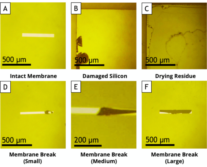
Figure 2: Optical microscope pictures of E-chips illustrating: (A) An intact SiN window that is necessary for the experiment. (B) A damaged silicon wafer at the edge of the E-Chip. This type of E-chips can be used if the damaged area is outside the wet area once the liquid cell is sealed (i.e., if the damage is outside the area defined by the O-rings). (C) Residues on the E-chip surface. If such residues do not leave after repeating the cleaning processes (see section 4.1), do not use the E-chip. (D to F) Damaged SiN windows (unusable E-chips). Please click here to view a larger version of this figure.
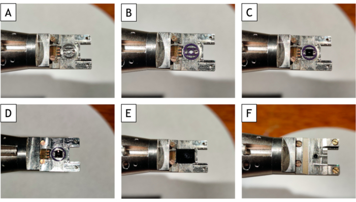
Figure 3: Photos of the step-by-step process of the loading of the liquid cell in the TEM holder. (A) Sample holder alone. (B) Put the gasket O-ring in the cavity. (C) Insert the small E-chip in gasket O-rings. (D) Put a drop of solution on the small E-chips. (E) Put the large E-chip over the small one. (F) Seal the whole liquid-cell by screwing the lid. Please click here to view a larger version of this figure.
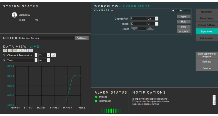
Figure 4: Screenshot of the heating software controlling the temperature of the liquid cell. Please click here to view a larger version of this figure.
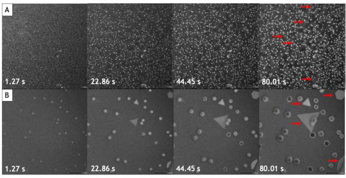
Figure 5: Low-magnification STEM HAADF image series of the growth of gold nanoparticles. (A) At 25 °C. (B) At 85 °C. The corresponding time is indicated in the bottom left corner of each image. The 2D nanostructures are indicated by red arrows. All images are acquired with the same electron dose rate of 3.4 electron·s-1·nm-2. Please click here to view a larger version of this figure.
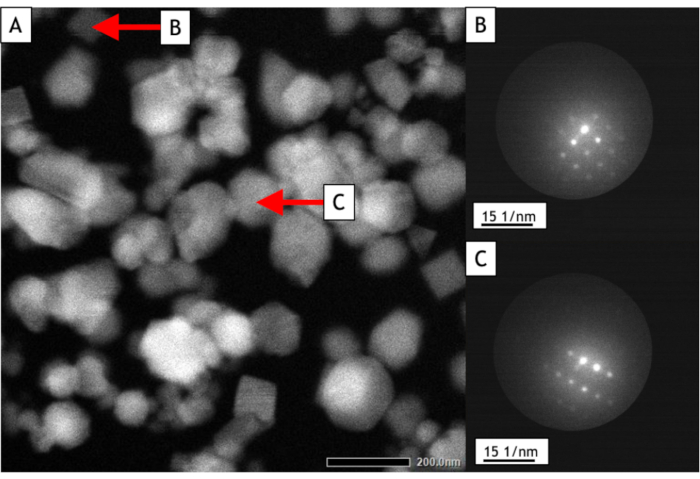
Figure 6: STEM nanodiffraction of single nanoparticles. (A) STEM image used to select the diffracting nanoparticles (the positions of the probe during diffraction acquisitions are indicated by red arrows). (B,C) Diffraction pattern of the two selected nanoparticles. Please click here to view a larger version of this figure.
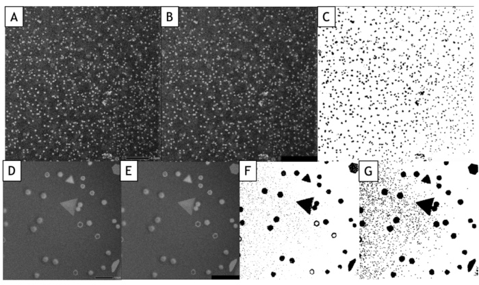
Figure 7: Data processing and analysis of STEM HAADF images using Fiji. The images were acquired 40 seconds after the beginning of the growth. (A to C) Image acquired at 25 °C. (D to G) Image acquired at 85 °C. (A,D) Raw STEM image. (B,E) Processed image (median filter). (C,F) Binary image. (G) A dilatation of the pixels is applied two times and the "Fill holes" process is then applied. Please click here to view a larger version of this figure.
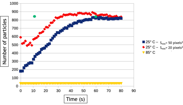
Figure 8: Graph representing the number of gold nanoparticles as a function of time at 25 °C and 85 °C. The two curves at 25°C are automatically measured with a minimal detection size (Smin) of 20 (red) and 50 (blue) pixels2. The green dots measured after 12 and 60 seconds of acquisition represent the number of nanoparticles counted manually on the video acquired at 25 °C. Please click here to view a larger version of this figure.
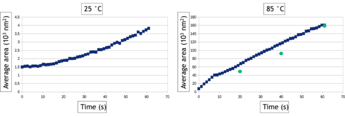
Figure 9: Graphs representing the average surface area of gold nanoparticles as a function of time for 25 °C and 85 °C. The green dots represent manual measurements of the average area of nanoparticles at given time points of the video acquired at 85° C. Please click here to view a larger version of this figure.
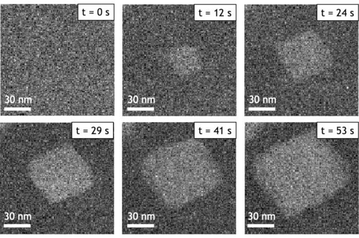
Figure 10: High-magnification STEM HAADF image series of the growth of single gold nanocube at 85 °C. This image series was acquired with an electron dose rate of 83.6 electron.s-1.nm-2. Please click here to view a larger version of this figure.
Discussion
The described protocol enables following the nucleation and growth of gold nanoparticles driven by radiolysis in a temperature-controlled liquid media. Combined with automated video processing, it allows measuring the effect of the temperature on key parameters of nanoparticle synthesis such as the density, the size, the shape and the atomic structure of nanoparticles. These valuable inputs allow evaluating the effect of the temperature on the nucleation and growth rates, detecting possible phase transitions and visualizing the faceting processes that dictate the final outcome of colloidal solutions. Together with the possibility to control the composition of the reactive media, temperature-controlled liquid cell TEM is another step towards the direct observation of the nucleation and growth processes of various nanostructures in realistic synthesis conditions. The interpretation of the results presented in this article and their comparison with nucleation and growth models will be discussed elsewhere. Here, we want to highlight several methodological aspects that must be considered to conduct relevant in situ TEM experiments.
First of all, it is crucial to identify the electron beam effects in the reaction media because they can drastically influence the results of the experiment. Here, as water radiolysis is the driving force of nanoparticle formation, the growth speed increases rapidly with the electron dose rate which will impacts the final shape of nano-objects11,15. Therefore, to study the effects of the temperature on the nucleation and growth of nanoparticles, it is necessary to compare growth experiments acquired with the same electron dose rate. In STEM mode, the electron dose rate corresponds to the beam current (in electron per second) divided by the image size (in nm2). Therefore, a constant electron dose rate implies to maintain the same beam current (i.e., same condenser aperture and same spot size) and the same magnification for each experiment. Quantifying the beam current of the imaging conditions using a CCD camera or a Faraday cup is important to interpret and reproduce the data. The magnification and resulting dose rate should be selected according to whether one wishes to visualize the growth of a large assembly of nanoparticles to extract statistically relevant results on the growth kinetics (Figure 5) or the growth mechanisms at the single nanoparticle scale to identify the preferential adsorption sites on the nanoparticle surfaces (Figure 10). If the nucleation and growth processes are too fast, particularly at high magnification, small condenser aperture and small spot size should be selected to minimize the dose rate. The nucleation and growth of nanoparticles can also slow down by reducing the concentration of metal precursor in the analyzed solution but note that the concentration of radiolytic products will increase with temperature. In a general manner, it is also important to take into account the electron irradiation history of the whole sample. Here, for example, if several growth experiments are rapidly performed in areas close to each other, the density of nanoparticles will decrease over time because the concentration of gold precursors in the studied area decreases. This effect can be minimized by separating the growth experiments both in space and time and by using the liquid-holder in flow mode.
Interface-tracking algorithms are extremely helpful to automatize the analysis of videos and extract quantitative results on the nucleation and growth of large nanoparticles assemblies. However, it is worth noting that the image-binarization step is always data specific, meaning that the filters and the data processing that must be applied on images to optimize the detection of the nanoparticle/liquid interface will vary from an experiment to another. Moreover, it is essential to compare the results of these automated analyses with manual measurements performed on a few images to optimize the image-processing workflow and to know its limitations. Here, for example, multiple scattering events in the increasingly thick 3D nanoparticles formed at high temperature induces a contrast inversion of their core after 30 seconds of observation because the angular broadening of scattered electrons results in a decrease of the collected signal in the angular range of the annular detector. To keep measuring the true surface area of these nanoparticles, we used a "fill holes" data process after the binarization of the image that fills the inner circle of ring shape contrasts (Figure 7F,G). However, we had to use a small dilatation of the objects to make sure that these ring shape contrasts are always fully connected. This latter step leads to a slight overvaluation of the mean surface area of nanoparticles in the automated measurements (Figure 9). Similarly, for the detection of nanoparticles, we have to define a minimal size of detected objects (Smim) to avoid detecting the noise, but this parameter affects the measured nucleation rate. As seen in Figure 8, the number of detected nanoparticles increase at the beginning of the experiment to reach a plateau. When Smin is large (50 pixels2 corresponding to 1543 nm2), automatic and manual measurements agreed on the level of this plateau (835 nanoparticles after 60 seconds) but the detection of nanoparticles is delayed in the automatic analysis since 835 nanoparticles are manually counted after only 12 s, but not automatically detected until later. This extended detection time leads to an undervaluation of the nucleation rate. Reducing Smin down to 20 pixel2 (i.e., 617 nm2) reduces the error on the nucleation time of the nanoparticle assembly but it leads to an overvaluation of the nanoparticle density particularly at the early stage of the experiments (Figure 8) which also affects the nucleation rate. The detection and the size and shape measurements of nano-objects with a very dynamical behavior and a low signal to noise ratio is a common challenge in liquid-phase TEM that can be further improved using other segmentation and denoising methods24 or machine learning approaches25.
Last but not least, the preparation of the liquid cell and the cleaning of the liquid holder must be very carefully performed to avoid contaminations of the reaction media.
In general, controlling the temperature of the sample during LCTEM analyses provides the opportunity to investigate thermal effects on chemical reactions that occur at the interface between solids and liquids. Therefore, we hope that the present method paves the way to other in situ TEM experiments designed to reveal the dynamics of hard, soft or biological materials in temperature-controlled liquid media.
Acknowledgements
We gratefully acknowledge the financial support of the Region Ile-de-France (convention SESAME E1845 for the JEOL ARM 200 F electron microscope installed at the University of Paris), the Labex SEAM (GLOIRE Project) and the CNRS (Defi Nano Program). We thank Madeline Dukes and Daniel Franck for sharing the schematics and the optical pictures of the liquid cells seen in figures 1 and 2.
Materials
| Name | Company | Catalog Number | Comments |
| 2100 Plus electron microscope | Jeol | ||
| Acetone | Merck | ||
| Air pistol | |||
| ARM 200F electron microscope | Jeol | ||
| Binoculars or optical microscope | |||
| Carbon tipped tweezers | |||
| Computer with heating software | Software by Protochips | ||
| Distlilled water | |||
| Dummy e-chips | Protochips | ||
| Gasket/O-rings | Protochips | ||
| Gold aqueous solution | Merck | 1 mM of HAuCl4 - Prepared beforehand | |
| Large liquid heating E-chip | Protochips | ||
| Methanol | Merck | ||
| One View camera | Gatan | ||
| Petri dish | Number : 2 | ||
| Plasma cleaner | Gatan | ||
| Poseidon Select | Protochips | Liquid cell holder | |
| Power supply Keithley 2450 | |||
| Protective gloves | |||
| Red PEEK tubing | Number : 3 | ||
| Screwdriver with torque | |||
| Small liquid E-chip | Protochips | 150 nm spacers | |
| STEM HAADF detector | Jeol | ||
| STEMx software | Gatan | ||
| Syringe | Number : 2 | ||
| Syringe pump | Harvard apparatus | Number : 2 | |
| Vacuum pump | Gatan |
References
- Willets, K. A., Van Duyne, R. P. Localized surface plasmon resonance spectroscopy and sensing. Annual Review of Physical Chemistry. 58 (1), 267-297 (2007).
- Dreaden, E. C., Alkilany, A. M., Huang, X., Murphy, C. J., El-Sayed, M. A. The golden age: gold nanoparticles for biomedicine. Chemical Society Review. 41, 2740-2779 (2012).
- You, H., Yang, S., Ding, B., Yang, H. Synthesis of colloidal metal and metal alloy nanoparticles for electrochemical energy applications. Chemical Society Review. 42, 2880-2904 (2013).
- Nikoobakht, B., El-Sayed, M. A. Preparation and growth mechanism of gold nanorods using seed-mediated growth method. Chemistry of Materials. 15, 1957-1962 (2003).
- Hubert, F., Testard, F., Spalla, O. Cetyltrimethylammonium bromid silver bromide complex as the capping agent of gold nanorods. Langmuir. 24, 9219-9222 (2008).
- Xia, Y., Xiong, Y., Lim, B., Skrabalak, S. E. Shape-controlled synthesis of metal nanocrystals: Simple chemistry meets complex physics. Angewandte Chemie International Edition. 48, 60-103 (2009).
- Zheng, Y., Zeng, J., Ruditskiy, A., Liu, M., Xia, Y. Oxidative etching and its role in manipulating the nucleation and growth of noble-metal nanocrystals. Chemistry of Materials. 26, 22-33 (2014).
- Xin, H. L., Zheng, H. In situ observation of oscillatory growth of bismuth nanoparticles. Nano Letters. 12 (3), 1470-1474 (2012).
- Wu, J., et al. Growth of Auau on Pt icosahedral nanoparticles revealed by low-dose in situ TEM. Nano letters. 15, 2711-2715 (2015).
- Ahmad, N., Wang, G., Nelayah, J., Ricolleau, C., Alloyeau, D. Exploring the formation of symmetric gold nanostars by liquid-cell transmission electron microscopy. Nano letters. 17, 4194-4201 (2017).
- Woehl, T. J., Evans, J. E., Arslan, I., Ristenpart, W. D., Browning, N. D. Direct in situ determination of the mechanisms controlling nanoparticle nucleation and growth. ACS Nano. 6, 8599-8610 (2012).
- Tan, S. F., et al. Intermediate structures of pt-ni nanoparticles during selective chemical and electrochemical etching. The Journal of Physical Chemistry Letters. 10, 6090-6096 (2019).
- Xin, H. L., Zheng, H. In situ observation of oscillatory growth of bismuth nanoparticles. Nano Letters. 12, 1470-1474 (2012).
- Aliyah, K., et al. Real-time in situ observations reveal a double role for ascorbic acid in the anisotropic growth of silver on gold. The Journal of Physical Chemistry Letters. 11 (8), 2830-2837 (2020).
- Alloyeau, D., et al. Unravelling kinetic and thermodynamic effects on the growth of gold nanoplates by liquid transmission microscopy. Nano Letters. 15 (4), 2574-2581 (2015).
- Gao, W., et al. Direct in situ observation and analysis of the formation of palladium nanocrystals with high-index facets. Nano Letters. 18 (11), 7004-7013 (2018).
- Liao, H. -. G., et al. Facet development during platinum nanocube growth. Science. 345, 916-919 (2014).
- Tan, S. F., et al. Real-time imaging of the formation of Au-Ag core-shell nanoparticles. Journal of the American Chemical Society. 138 (16), 5190-5193 (2016).
- Khelfa, A. Selective shortening of gold nanorods: when surface functionalization dictates the reactivity of nanostructures. Nanoscale. 12, 22658-22667 (2020).
- Schneider, N. M., et al. Electron-water interactions and implications for liquid cell electron microscopy. Journal of Physical Chemistry C. 118, 22373-22382 (2014).
- Ahmad, N., Le Bouar, Y., Ricolleau, C., Alloyeau, D. Growth of dendritic nanostructures by liquid-cell transmission electron microscopy: a reflection of the electron-irradiation history. Advanced Structural and Chemical Imaging. 2, 9 (2016).
- Khelfa, A., et al. Structural analysis of single nanoparticles in liquid by low-dose STEM nanodiffraction. Micron. 116, 30-35 (2019).
- Ahmad, N., Wang, G., Nelayah, J., Ricolleau, C., Alloyeau, D. Driving Reversible Redox Reactions at Solid/Liquid Interfaces with the Electron Beam of a Transmission Electron Microscope. Journal of Microscopy. 269, 127-133 (2018).
- Schneider, N. M., Park, J. H., Norton, M. M., Ross, F. M., Bau, H. H. Automated analysis of evolving interfaces during in situ electron microscopy. Advanced Structural and Chemical Imaging. 2, (2016).
- Yao, L., Ou, Z., Luo, B., Xu, C., Chen, Q. Machine learning to reaveal nanoparticle dynamics from liquid-phase TEM videos. ACS Central Science. 6, 1421-1430 (2020).
Explore More Articles
This article has been published
Video Coming Soon
ABOUT JoVE
Copyright © 2024 MyJoVE Corporation. All rights reserved