
A subscription to JoVE is required to view this content. Sign in or start your free trial.
Method Article
A 3D-printed Chamber for Organic Optoelectronic Device Degradation Testing
In This Article
Summary
Here, we present a protocol for the design, manufacture, and use of a simple, versatile 3D-printed and controlled atmospheric chamber for the optical and electrical characterization of air-sensitive organic optoelectronic devices.
Abstract
In this manuscript, we outline the manufacture of a small, portable, easy-to-use atmospheric chamber for organic and perovskite optoelectronic devices, using 3D-printing. As these types of devices are sensitive to moisture and oxygen, such a chamber can aid researchers in characterizing the electronic and stability properties. The chamber is intended to be used as a temporary, reusable, and stable environment with controlled properties (including humidity, gas introduction, and temperature). It can be used to protect air-sensitive materials or to expose them to contaminants in a controlled way for degradation studies. To characterize the properties of the chamber, we outline a simple procedure to determine the water vapor transmission rate (WVTR) using relative humidity as measured by a standard humidity sensor. This standard operating procedure, using a 50% infill density of polylactic acid (PLA), results in a chamber that can be used for weeks without any significant loss of device properties. The versatility and ease of use of the chamber allows it to be adapted to any characterization condition that requires a compact-controlled atmosphere.
Introduction
Organic and perovskite optoelectronic devices, solar cells, and light-emitting diodes based on π-conjugated semiconducting organic molecules and organometal halides are a rapidly growing field of research. Organic light-emitting diodes (OLEDs) are already a major technological element in lighting and displays1, and organic photovoltaics have begun to achieve efficiencies that make them competitive with amorphous silicon2. The recent rapid advancement of perovskite-based devices for light absorbing and light-emitting applications3,4,5 suggests that low-cost, easily processed devices are likely to soon find widespread deployment. However, all of these technologies suffer from a sensitivity to atmospheric contaminants, particularly moisture and oxygen, which limits their effective lifetimes6,7,8,9.
For researchers studying such systems, it can be useful to have an adaptable, easy-to-use, portable, and reusable chamber to protect such sensitive materials or to expose them to contaminants in a controlled manner10,11. Though it is possible to use a glovebox for the characterization of air-sensitive devices, these large, expensive, and fixed-location, inert environments may be incompatible with the wide range of characterization that might be required. To provide a portable alternative, Reese et al.10 proposed a small metal chamber based on a standard vacuum flange suitable for the electrical and optical characterization of organic devices. We have adapted this design, making it cheaper and more versatile by using 3D-printing to produce the chamber components. The use of 3D-printing, rather than machining, allows for rapid, cost-effective adjustments to changing sample or environmental requirements while maintaining the utility of the basic design. In this contribution, we outline the procedure to make such a chamber, and use it to extract the current-voltage characteristics of an organic diode device.
A good encapsulation of organic and perovskite devices should have WVTRs of 10-3 - 10-6 g/m2/day for long-term device stability12,13, to ensure little water ingress into the organic device even in very harsh conditions. As this chamber is designed to be a controlled environment for testing purposes rather than a long-term storage or encapsulation method, the requirements for an effective chamber are not as strict. The chamber should be able to maintain the device properties within a reasonable timeframe to perform characterization experiments. The standard operating procedure of using PLA results in a chamber which can be used for several days or even weeks with an incorporated gas flow, without a significant loss of the device properties.
Changing the materials, or even the shape and size of the chamber body can drastically affect the penetration of contaminants from the air into the chamber. Therefore, the ingress of moisture and oxygen needs to be carefully monitored for each design to determine the efficacy of the chamber. We, additionally to the fabrication of the chamber, outline a simple procedure for determining the WVTR of the chamber, using a commercially available humidity sensor, to establish a timeframe for the use of the chamber for experimentation.
Such a simple, yet versatile chamber allows for multiple types of experiments to be performed. They can act as inert atmosphere environments outside the glovebox, suitable for electrical and optical characterizations through the electrical feedthrough ports and window. Their portability allows them to be used with standard electrical characterization equipment outside the lab where they were manufactured, which is useful in round robin testing for reliability14 or to obtain certified measurements of the device performance15. These chambers are also particularly useful for studying the effects of the introduction of contaminants for controlled degradation tests, with simple modifications. The use of 3D printing allows a significant, rapid adaptability to changing device layouts, sizes, or testing requirements.
Access restricted. Please log in or start a trial to view this content.
Protocol
1. The 3D Print Chamber Parts
Note: All printer preparation, “slicer” software settings, and print parameters were specific to the printer indicated in the Table of Materials. There is a wide array of 3D printers, each with their own set of preparation steps and optimal parameters. There is also a wide array of colors possible for the polymer filament used for the printed parts. It is not required to use the same plastic for each part.
- Select the corresponding .stl files based on the desired chamber configuration.
Note: These configurations are detailed in Figure 1, along with an exploded view of one complete chamber configuration. - Set up the slicing software to convert the .stl files to .gcode files that the printer will read.
- Download the slicing software listed in the Table of Materials.
- Select the printer in use by navigating to Other and find the printer in use.
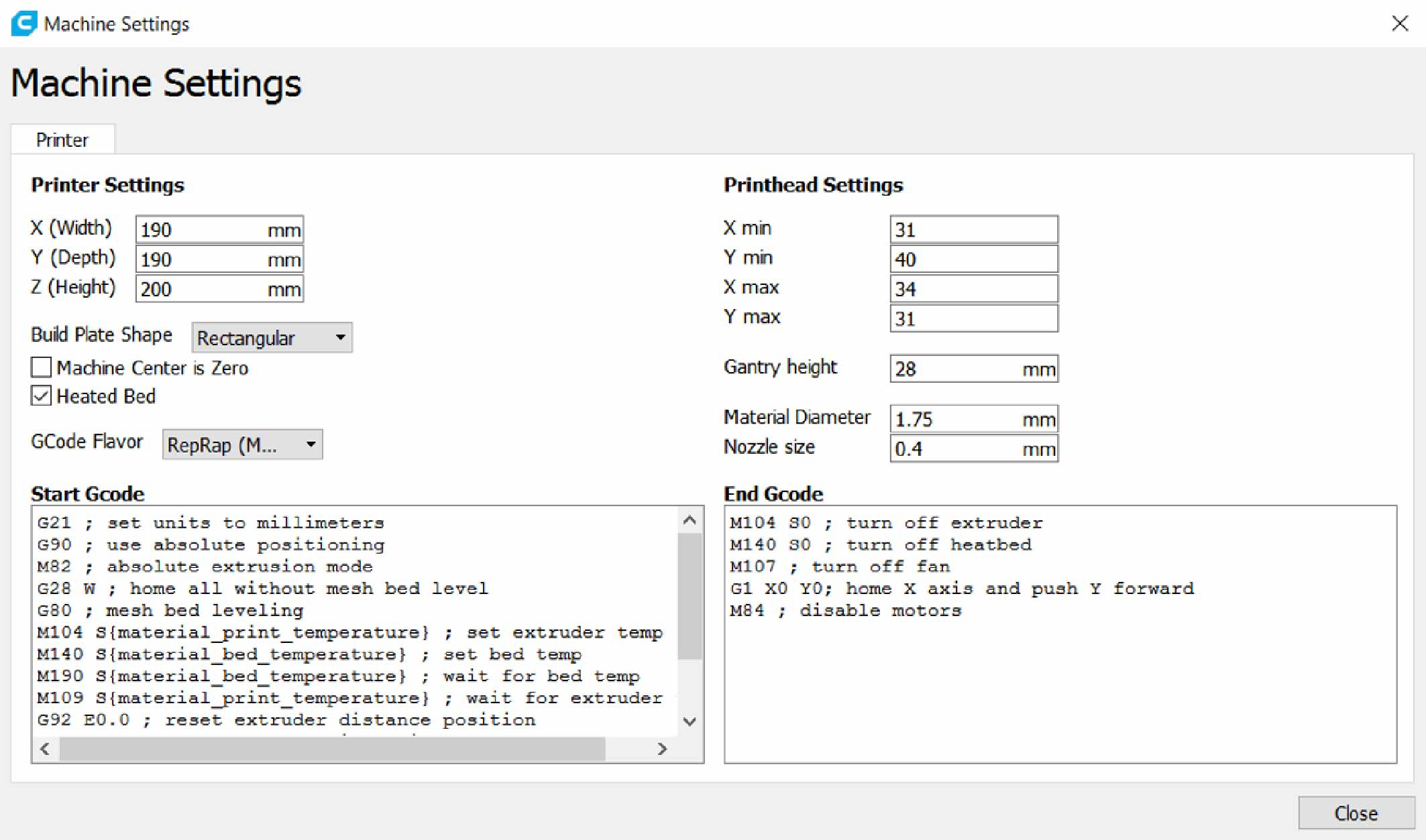
- Navigate to Settings > Printer > Manage Printers > Machine Settings and change the settings as shown in Figure 2.
- Convert the .stl file to a .gcode file with user-desired parameters with the slicing software.
- Save the converted .gcode file to the SD card and insert it into the 3D printer.
- Prepare the 3D printer for use.
- Cover the printing bed with blue masking tape. Ensure there are no rips, air bubbles, or uneven surfaces by running a credit card-type object over the surface.
- Level the printer bed if necessary. The method differs per printer and can be researched.
- Navigate to Print from SD card on the 3D printer display and select the desired file.
Note: The printer will, at first, heat up its bed and nozzle, and then the print will begin. - Repeat steps 1.3 - 1.6 for each part to be printed.

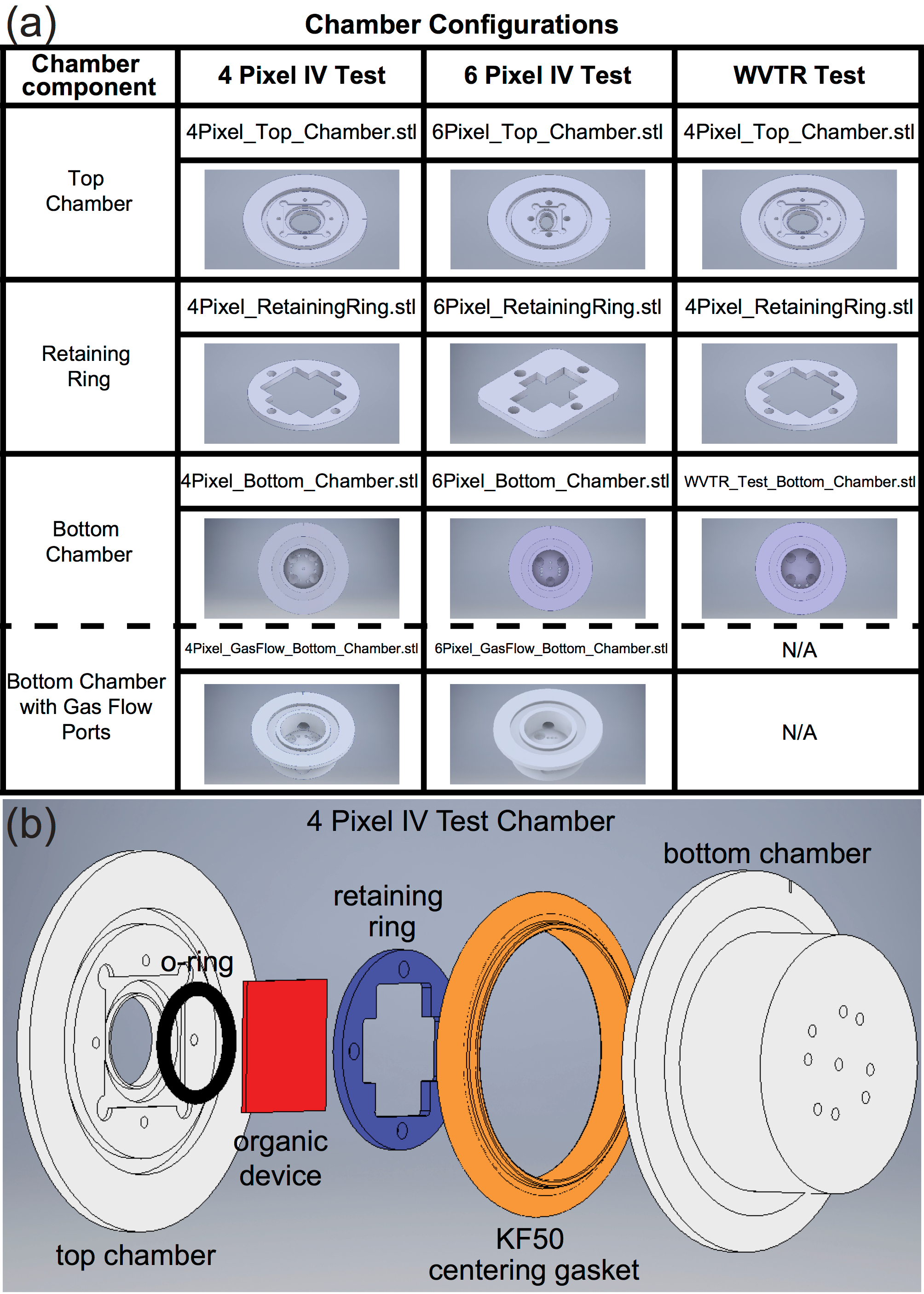
Figure 1: A configuration table with an exploded view of the test chamber. (a) This table shows the .stl files for various chamber configurations. The rows show 3D-rendered schematics of the variations on each chamber part to be printed. The columns show the necessary parts to complete a single chamber. Note that a chamber will have either a bottom chamber or a bottom chamber with gas ports, not both. (b) This panel shows an exploded CAD view of a printed chamber for a 4-pixel IV test configuration. Note that the O-ring, the organic device, and the KF50-centering gasket are not 3D printed. Please click here to view a larger version of this figure.

Figure 2: 3D printer settings. This is a screenshot of the required machine settings in the slicing software to produce the 3D-printed parts for the chambers. Please click here to view a larger version of this figure.
2. The Top Chamber Assembly
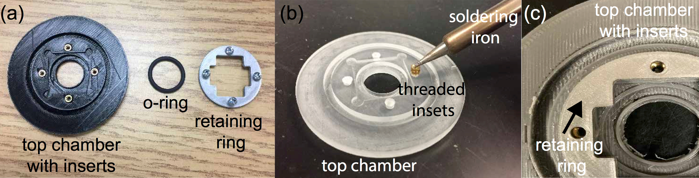
- Add threaded inserts to top chamber (see Figure 3b for information on how to apply threaded inserts).
- Drill 4 tapping holes of 0.404 cm in diameter (size 21 imperial) to a depth of 0.397 cm (5/32 in) in the 4 pilot holes in the underside of the printed top chamber (see Figure 1a).
- Place a brass-tapered threaded insert with a #4-40 thread size (0.248 cm in diameter) into the drilled hole with the smaller diameter facing down.
- Turn on a soldering iron. When heated to around 330 - 350 °C, press the soldering iron tip to the threaded insert and apply nominal pressure as the insert heats the plastic to allow it to slide into the prepared holes. Keep applying pressure (ensuring the insert is moving straight down) until the top face of the insert and the underside face of the top chamber are about 1 mm apart.
- Lightly press the edge of a straightedge against the top face of the insert while the plastic is still hot to ensure it is flush with the underside face of the top chamber. Allow 1 min for the plastic to cool before continuing.
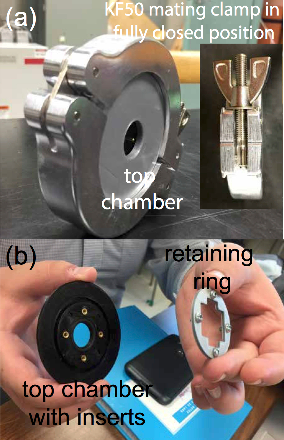
- Ensure the alignment of the inserts by placing the retaining ring over the insert and checking to see if the holes line up. See Figure 3c.
- Repeat the procedure of steps 2.1.2 - 2.1.5 for all 4 inserts.
- Insert and press the size-116 butyl O-ring into the circular groove in the underside of the top chamber.
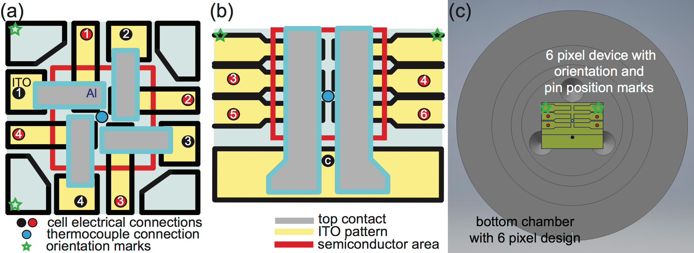
- Place the organic device on top of the O-ring (see Figure 4 for the details of 2 possible pixel patterns).
Note: A single organic device can be made up of a number of individual diodes that can be measured independently. These are referred to as “pixels.” The patterns in Figure 4 represent the orientation of the organic device as it should be placed in the top chamber. The notch on the side of the chamber should be to the left of the organic device (4-pixel) or below the organic device (6-pixel) (relative to the orientation marks on the patterns in Figure 4). - In a glovebox environment, fasten the retaining ring to the top chamber by screwing the four 4-40 thread screws (0.248 cm in diameter, 0.478 cm in length) through the retaining ring into the threaded inserts. Press the device between the retaining ring and the O-ring. Take extreme care not to crack the device by screwing the screws incrementally, going one-eighth turn each pass around.
Note: To guarantee a sufficient seal, check that the O-ring is pressed against the device all around with a 15 - 25% compression.

Figure 3: The assembling of the top chamber. (a) This panel shows a disassembled 4-pixel top chamber. (b) This panel shows the application of threaded inserts in the top chamber using a soldering iron. (c) This panel shows partially assembled top chamber components showing the alignment of the retaining ring to the top chamber (note that the O-ring and the screws are not shown for clarity). Different colors of PLA plastic were used for the printing of various parts; these have no effect on the performance of the chamber. Please click here to view a larger version of this figure.

Figure 4: Possible device pixel patterns for a pin layout. These panels show the layout of the organic solar cell or light-emitting diode device used for designating the contact pin positions for (a) a 4-pixel and (b) a 6-pixel IV test chamber configuration. Each pixel is numbered with a reference to the orientation marks (green stars) for their correct placement in the chamber. Black and red circles represent the cathode and anode contacts (i.e., pin positions), respectively. Note that for the 6-pixel configuration, the top two pixels are masked by the opening in the top chamber and not numbered as only four pixels can be tested under illumination or emission conditions. (c) This panel shows the orientation of a 6-pixel device relative to the 6-pixel bottom chamber with its pin positions indicated. Please click here to view a larger version of this figure.
- Leave the assembled top chamber in a glovebox environment for ≥ 24 h to allow any moisture absorbed by the chamber to escape from the material. Continue with step 3 while waiting.
3. The Bottom Chamber Assembly
Note: Only follow step 3.1 if a configuration with a bottom chamber with gas flow ports is needed.
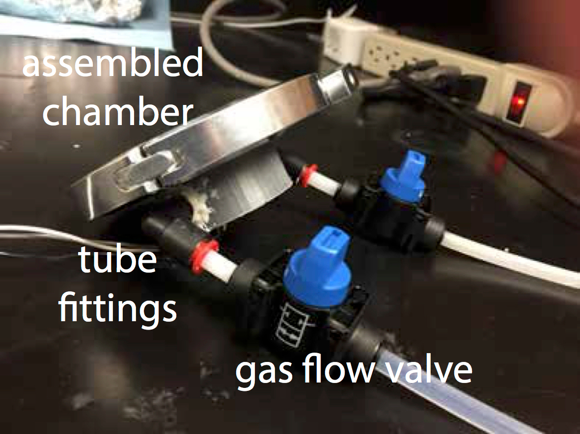
- Add push-to-connect pneumatic connectors for an inert gas flow to the bottom chamber with gas flow ports (see Figure 5).
- Using a 1/8 in-sized National Pipe Thread (NPT) tap with a hand T-wrench, tap both holes located on the side of the bottom chamber with the gas flow ports. Ensuring that the hole to be tapped is vertical and the chamber is securely held in place, place the tap in the hole.
- Using the T-wrench attached to the tap, slowly twist the wrench clockwise, ensuring that the tap remains vertical and lined up with the hole as the threads are formed. Every 5 turns, twist the wrench counter-clockwise one full turn, and then twist another 5 turns, repeating until a thread is cut to the bottom of the hole.
- Wrap the Teflon tape around the 2-pneumatic push-to-connect connectors by wrapping the tape counter-clockwise around the threads (when viewing the fitting from above as it is screwed in) 2x.
Note: For more information, please refer to a machinists’ tapping guidebook. - Screw the pneumatic connectors into the tapped holes, using a wrench to tighten them. Take care not to overtighten and crack the plastic.
- Apply low-pressure epoxy around the seated fittings. On a piece of foil, use a popsicle stick to mix 2-part base resin with 1-part hardener (both are included). This mixture is the epoxy.
- Using a toothpick, apply a layer of epoxy in and around the space between the bottom chamber with the gas flow ports and the fittings. Allow the epoxy to sit for 1 - 2 h for the resin to harden at 25 °C. For a full curing, allow the epoxy to rest for 24 h at 25 °C. Ensure that the set resin is white and solid when pressed.
CAUTION: Epoxy hardener and epoxy resin cause burns and irritation of the eyes and skin. Epoxy may cause an allergic skin or respiratory reaction. It may cause respiratory tract irritation. It may be harmful if swallowed or absorbed through the skin. Ensure adequate ventilation and avoid any contact with skin and clothing. Do not breathe in the vapor. Wear eye protection and gloves when handling epoxy. - Connect the pneumatic push-to-connect connectors with the manually operated push-to-connect valves with 2 cm pieces of Teflon tubing. The diameter of the tubing should match that which is required by the push-to-connect connector used.

Figure 5: An assembled chamber with gas ports. This panel shows a fully assembled chamber including a bottom chamber with gas ports. The push-to-connect gas ports embedded in the available holes in the chamber are attached to tubing with gas flow control valves to control the introduction of gas. Note that the contact pins are omitted for clarity. Please click here to view a larger version of this figure.
- Add electrical contact pins to the bottom chamber for a current voltage (IV) measurement (see Figure 6).
- Insert 6 - 7 mm of the narrow end of a pogo pin into the female end of a solder cup. The combination of these 2 parts is known as a contact pin. Using solder helping hands, suspend both parts of the contact pin horizontally.
- Turn on the soldering iron. When heated to around 330 - 350 °C, touch the iron to the connection region between the pogo pin and the solder cup.
- While still touching the iron to the area, press the solder to the connection region. If it has heated enough, the solder will melt. Ensure there is a thin layer of solder covering the area between the two parts all the way around the exterior of the contact pin. Ensure the solder is smooth with no bumps. See Figure 6b.
- Slide the contact pin into 1 of the holes in the underside of the bottom chamber. Slide the contact pin so that 2.2 cm of the solder cup end is protruding from the bottom of the bottom chamber.
Note: The solder cup should stick out the bottom of the bottom chamber while the pogo pin should be towards the inside of the bottom chamber. - For sealing, cover the region where the contact pin was inserted into the plastic with low-pressure epoxy suitable for vacuum applications. On a piece of foil, use a popsicle stick to mix 2-part resin with 1-part hardener until the mixture appears uniform.
- Using a toothpick, apply the epoxy around the contact pin and hole to eliminate the possibility of air ingress. Allow 1 - 2 h for the resin to harden at 25 °C. For a full curing, allow the epoxy to rest for 24 h at 25 °C. Ensure that the set resin is white and solid when pressed.
CAUTION: Epoxy hardener and epoxy resin cause burns and irritation of the eyes and skin. Epoxy may cause an allergic skin or respiratory reaction. It may cause respiratory tract irritation. It may be harmful if swallowed or absorbed through the skin. Ensure adequate ventilation and avoid any contact with skin and clothing. Do not breathe in the vapor. Wear eye protection and gloves when handling epoxy. - Repeat steps 3.2.1 - 3.2.6 to add the correct number of contact pins to the bottom chamber to fill the holes.
- Place the assembled bottom chamber into a glovebox environment and leave it for at least 24 h.
Note: This is to allow any moisture absorbed by the chamber to escape from the material.

Figure 6: A complete, assembled bottom chamber. (a) This panel shows an assembled bottom chamber for a 4-pixel IV test configuration with the contact pins seated using low-pressure epoxy suitable for vacuum applications. The brown O-ring (KF50)-centering ring gasket is used to ensure a tight fitting with the top chamber. (b) This panel shows a solder cup and pogo pin after soldering. (c) This panel shows a close-up of set epoxy, showing the correct seating of the contact pin in the bottom chamber holes. Please click here to view a larger version of this figure.
4. The Final Assembly
Note: This assembly is to be done within a glovebox environment after both the assembled top and the bottom chamber have been inside the glovebox for ≥ 24 h.
- Attach a KF50-centering gasket to the bottom chamber, as shown in Figure 6.
- Place the top chamber on the bottom chamber, with the smooth side of the top chamber facing upwards and align the notches on both chamber parts to ensure proper contact with the organic device. See Figure 1 for an exploded view of the whole chamber.
- Secure the 2 chamber parts together using the KF50 clamp.
- Unfasten the wingnut on the clamp and place the clamp around the edge of the combined bottom chamber and top chamber.
- Using the inset of Figure 7 for a clear representation, twist the wingnut as far as it can go to fasten the bolt, ensuring a tight seal around the 2 half-chambers. Leave the completed chamber in the glovebox until the software has been configured as detailed in step 5.

Figure 7: An assembled, complete test chamber. (a) This panel shows a fully assembled 4-pixel IV test chamber with a KF50 cast clamp ensuring a tight fit between the bottom and top chamber. The inset shows another angle of the KF50 clamp closed in the maximum tightness position. (b) This panel shows an assembly of the 4-pixel top chamber with the retaining ring (note that the O-ring is already mounted in the top chamber). Other chamber configurations are assembled in the same way. Please click here to view a larger version of this figure.
5. Conduct IV Measurements of the Individual Pixels on the Device
Note: This section details the procedure used to generate the data shown in the Representative Results. The source-measurement unit (SMU) and the Zero Insertion Force (ZIF) test board used are listed in the Table of Materials. However, any method of chamber connection to an SMU to collect current-voltage data can be used. All IV measurement steps were conducted on a Windows machine. “Pixel” refers to a single diode on the organic device.
- Download and install the provided Python IDE.
- Connect a BNC cable from the SMU 1 channel located on the SMU to the ZIF test board.
- Connect the power supply to the SMU and connect it to a computer via a USB 2.0 cable.
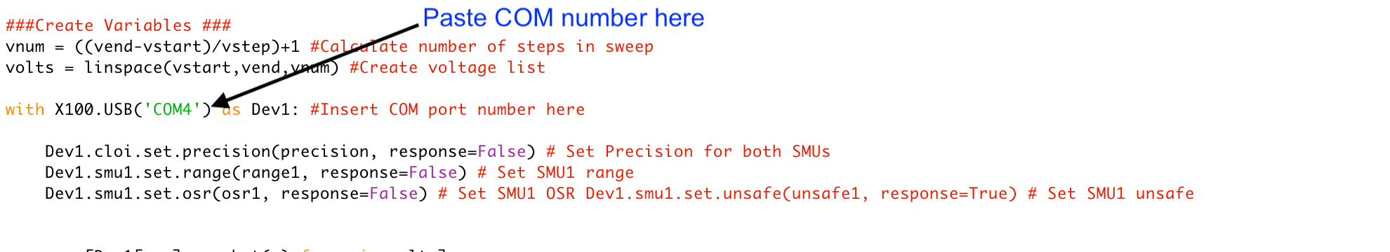
- Identify the correct COM port/serial port ID that corresponds to the connected SMU.
- For Windows devices, check which COM port corresponds to the connected SMU in the Device Manager. Take note of the COM number.
- Open the BasicIV.py Python script.
- Paste the COM port (Windows) in the indicated line of code in BasicIV.py as seen in Figure 8.
Note: By default, the program will output data in the current working directory.

Figure 8: The IV measure in Python. This is a screen shot of the BasicIV.py Python script with the COM port location indicated. Please click here to view a larger version of this figure.
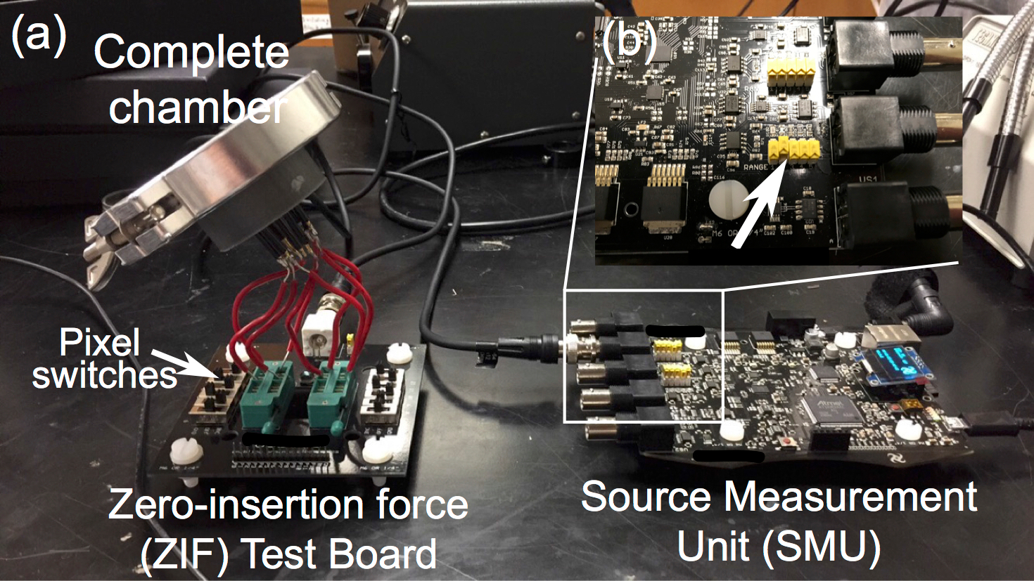
- On the SMU, toggle the Range switch labeled “2” located near the SMU 1 channel to the ON position. See Figure 9b.
- Remove the fully assembled chamber from the glovebox environment.
- Bridge the connection between the contact pins and the ZIF test board using a method of choice (see Figure 9).
Note: For this setup, a custom adaptor was made to bridge the connection between the contact pins and the ZIF test board when running IV measurements. This method can vary, as long as the connections are sufficient and add negligible resistance. - Switch the cathode pin to Ground and the anode pin to BNC for only 1 pixel at a time, ensuring the rest of them are switched OFF.
- Run BasicIV.py.
Note: When the measurement is completed, files of results and a plot of V0 versus I0 will be produced in the previously selected file path. - Repeat steps 5.10 and 5.11 for each pixel on the device using the pixel switches shown in Figure 9 to measure the IV for each pixel.

Figure 9: The IV measurement set-up. (a) This panel shows a fully assembled chamber connected to the zero-insertion force (ZIF) test board and source measurement unit (SMU) for an IV measurement testing. (b) This panel shows the range switch "2" set in the ON position to correctly connect the device to the SMU for the measurement. Please click here to view a larger version of this figure.
6. Assemble the Chamber for WVTR Testing
- Add an internal humidity sensor to the WVTR test chamber for determining the WVTR.
- Solder 3 wires to the internal humidity sensor as shown in Figure 10c: 5 V (red), ground (green), and data (yellow). Ensure they are of sufficient length (approximately 15 cm).
- Feed internal humidity sensor wires through the holes at the bottom of the WVTR test bottom chamber.
- Using a toothpick, apply low-pressure epoxy around the wires inside and outside the bottom chamber as well as in any openings. On a piece of foil, use a popsicle stick to mix 2-part resin with 1-part hardener until the mixture appears uniform.
- Apply the epoxy around the wire and hole to eliminate the possibility of air ingress. Allow 1 - 2 h for the resin to harden at 25 °C. For a full curing, allow the epoxy to rest for 24 h at 25 °C. Ensure that the set resin is white and solid when pressed.
CAUTION: Epoxy hardener and epoxy resin cause burns and irritation of the eyes and skin. Epoxy may cause an allergic skin or respiratory reaction. It may cause respiratory tract irritation. It may be harmful if swallowed or absorbed through the skin. Ensure adequate ventilation and avoid any contact with skin and clothing. Do not breathe in the vapor. Wear eye protection and gloves when handling epoxy.
- Repeat step 2 to assemble a top chamber, replacing the device with a piece of glass the same size and thickness as the device that the chamber would be enclosing.
Note: If a top chamber is already assembled, then it may be used for this purpose. Since no device is being measured, to mimic the conditions of a device, a piece of glass is used to seal the top chamber’s optical opening. - Leave the test bottom chamber, assembled top chamber, and KF50-centering ring unassembled in an oxygen-/moisture-free environment (glovebox) for 24 h to ensure an initial condition of 0% internal relative humidity.
- Repeat step 4 to fully assemble a chamber built to measure the WVTR inside the glovebox, as shown in Figure 10a.

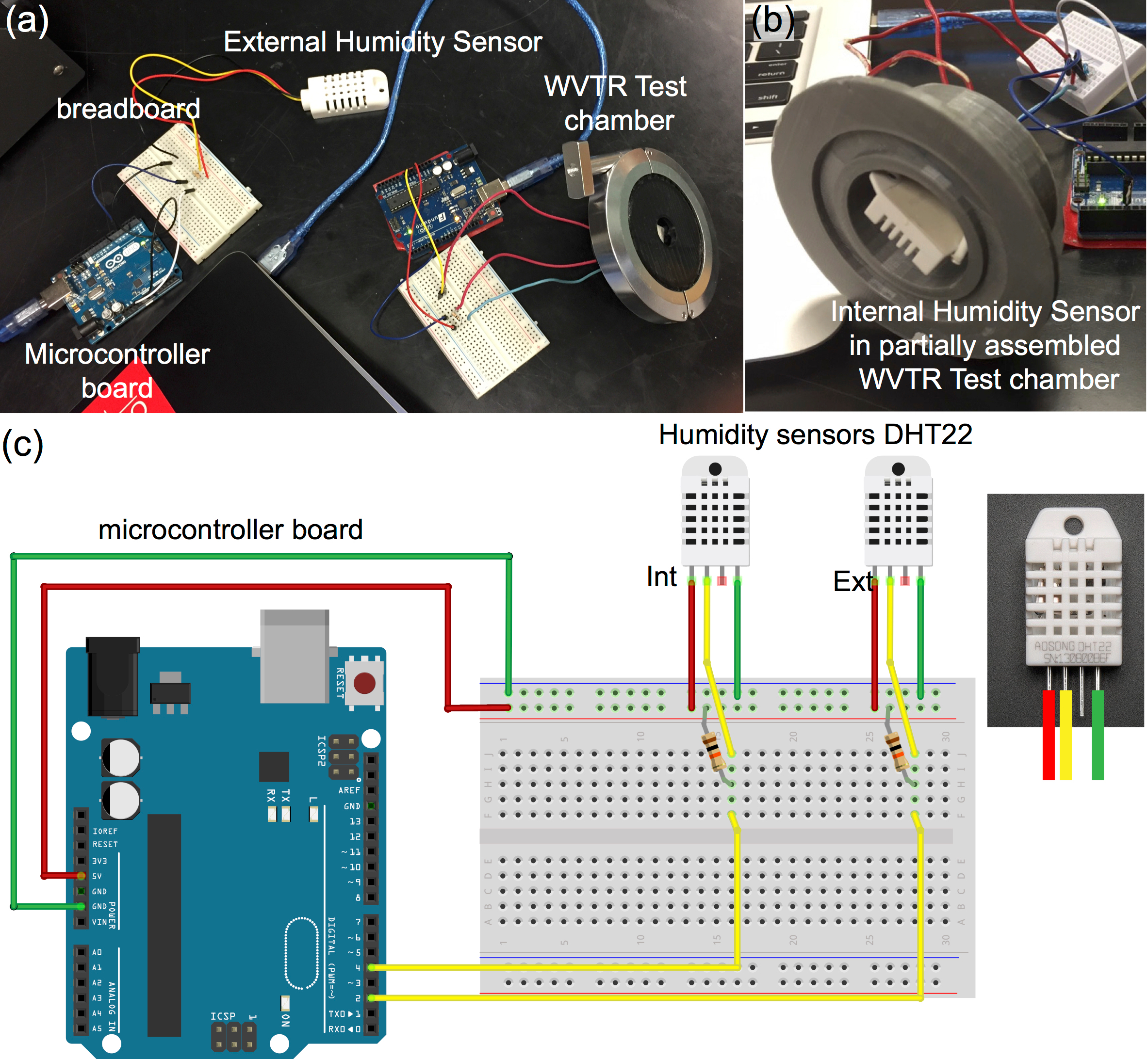
Figure 10: The humidity testing setup. (a) This panel shows a completely assembled WVTR test chamber wired to internal and external DHT22 humidity sensors using a breadboard jumper to a microcontroller. (b) This panel shows the DHT22 humidity sensor inside the WVTR test bottom chamber. Note that the wires are fed through the bottom chamber and are held in place with low-pressure epoxy. (c) This panel shows a schematic of the internal and external humidity sensor DHT22 and a microcontroller board wiring diagram using a single breadboard (for convenience). The sensor is connected to the microcontroller pins "5 V" (red) and "GND" (green) to provide power to the sensor. The data output from the sensor (yellow) connects to the pins in "DIGITAL" [2 for the internal (INT) sensor and 4 for the external (EXT) sensor] with a 10 kΩ resistor. The inset shows a DTH22 sensor with the correct pin wiring: 5V (red), ground (green), and data (yellow). Please click here to view a larger version of this figure.
7. Conduct a Humidity Measurement to Determine the WVTR
- Download the microcontroller board software and any Python 2.7.12 IDE on a compatible computer.
- Open Python file Run_WVTR_Test.py.
- Plug in the microcontroller to the computer via a USB A-B cable.
- Install the library to allow the output of the data to a spreadsheet.
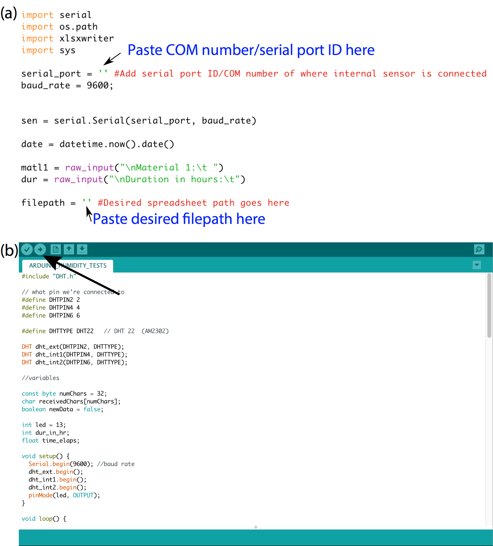
- Repeat step 5.4 to determine the COM number of the connected microcontroller. Copy and paste this into the Python code as shown in Figure 11a.
- Identify desired file path for raw data spreadsheets and enter it into the Python code as shown in Figure 11a.
- Open the microcontroller file ARDUINO_HUMIDITY_TESTS.ino.
- Under the Tools tab, select the appropriate microcontroller as the board. Under the Tools tab again, select the port as determined in step 7.5.
- Verify and upload the microcontroller code to the microcontroller by clicking the icon in the top left of the window as seen in Figure 11b.
- Wire the circuit as shown in Figure 10c; connect the 5 V (red), ground (black), and signal (yellow) wires of the external (EXT) humidity sensor to their respective locations. Omit the internal sensor (INT) until step 7.12 since it is located in the completed chamber, as shown in Figure 10b.
- Remove the assembled chamber from the glovebox.
- Immediately wire the internal sensor in the chamber to the microcontroller board as shown in Figure 10c.
- Run the Python script and follow the prompts that appear in the Python shell.
- Type in the material of the chamber.
- Type in the duration in hours. Bracket the number with an underscore. For example, if 6 h is desired, then type “_6_”.
Note: The test should begin and create .xlsx files in the path location specified within the script when the test is complete. Do NOT allow the sensors to disconnect from the setup. The test must be restarted if this happens. The microcontroller code for the WVTR measurement was adapted from the default program provided by the supplier. The Python code that runs the IV measurement was adapted from the code supplied by the manufacturer of the ZIF test board.

Figure 11: A water vapor transmission rate screenshot. These panels show (a) a screen shot of the Run_WVTR_Test.py Python script with (b) the COM port location indicated. Please click here to view a larger version of this figure.
Access restricted. Please log in or start a trial to view this content.
Results
Current-voltage Measurements:
This chamber is designed to allow for the testing of an air-sensitive diode device, such as an organic or perovskite solar cell or a light-emitting diode. It can act as a reusable, temporary encapsulation or as a method of introducing contaminants to perform controlled degradation testing. The current density-voltage (JV) curves shown here were measured using a ZIF test board attach...
Access restricted. Please log in or start a trial to view this content.
Discussion
The critical steps in recreating this experiment include the printing of the chambers to avoid cracks, gaps, or poor in-fill characteristics which can decrease the WVTR, sealing the chamber to prevent any ingress of moisture and oxygen by tightening the KF50 clamp to achieve a full sealing between the top and bottom chambers, using a vacuum-rated low-pressure epoxy around the contact pins or any feedthroughs to prevent any leaking, and creating a seal between the sample and the top chamber using a proper O-ring placement...
Access restricted. Please log in or start a trial to view this content.
Disclosures
The authors have nothing to disclose.
Acknowledgements
The authors acknowledge Peter Jonosson and the Lyons New Media Centre for the 3D printing of the chambers. This research was supported by 436100-2013 RGPIN, ER15-11-123, the McMaster Dean of Engineering Excellence Undergraduate Summer Research Award, and the Undergraduate Research Opportunities Program.
Access restricted. Please log in or start a trial to view this content.
Materials
| Name | Company | Catalog Number | Comments |
| ORION DELTA DESKTOP 3D PRINTER RTP | SeeMeCNC | 87999 | Known in Report As: 3D Printer |
| 1.75 mm PLA Filament | SeeMeCNC | 50241 | Known in Report As: PLA |
| Somos® WaterShed XC 11122 chamber | Somos | printed at Custom Prototypes, Toronto. | https://www.dsm.com/products/somos/en_US/products/offerings-somos-water-shed.html Known in Report As: Water resistant polymer |
| CURA | CURA | https://ultimaker.com/en/products/cura-software Known in Report As: slicing software | |
| Soldering iron with 600° F tip | Weller | WTCPT | |
| Xtralien X100 Source Measure Unit | Ossila | E561 | Known in Report As: SMU |
| ZIF Test Board for Pixelated Anode Substrates | Ossila | E221 | Known in Report As: Zero insetion force/ZIF Test Board; |
| BNC Cable | |||
| Generic USB A - B | |||
| Generic USB A - Micro | |||
| #12 O-Ring | Source unkown Known in Report As: o-ring | ||
| 116 Butyl O-Ring | Global Rubber Products | 116 VI70 | Bought in-store Known in Report As: o-ring |
| Retaining ring | McMaster | NA | 3D printed in-house |
| Bottom Chamber | McMaster | NA | 3D printed in-house |
| Top Chamber | McMaster | NA | 3D printed in-house |
| KF50 Cast Clamp (Aluminum) | Kurt J. Lesker | QF50-200-C | |
| KF50 Centering Ring (Aluminum) | Kurt J. Lesker | QF50-200-BRB | |
| Sn60/Pb40 Solder | MG Chemicals | 4895-2270 | |
| #4-40 x 3/16" machine screw | Hardware store | ||
| #4-40 IntThrd Brass TaperSingleVane Insert For Thermoplastic | Fastenal | 11125984 | Fastenal requires to be affiliated with company/university Known in Report As: #4-40 brass tapered threaded insert |
| Varian Torr Seal Vacuum Equipment High Vacuum Epoxy | Vacuum Products Canada Inc. | Known in Report As: low-pressure epoxy | |
| Smiths Interconnect/IDI Contact Probes HEADED RADIUS | Mouser Electornics | 818-S-100-D-3.5-G | Known in Report As: pogo pin |
| Smiths Interconnect/IDI Contact Probes Receptacle Solder Cup | Mouser Electornics | 818-R-100-SC | Known in Report As: solder cup |
| 1/4" Teflon Tubing | Hardware store | ||
| Teflon tape | Hardware store | ||
| 1/4" Tube x 1/8" Male NPT Nickel Plated Brass Push-to-Connect Connector | Fastenal | 442064 | Not the same ones used for this study, but are fuctionally equivalent Known in Report As: push-to-connect pneumatic connector |
| 1/8" NPT Tap and T-wrench | Hardware store | ||
| 1/4" Tube Push-to-Connect Manually Operated Valves | Fluidline | 7910-56-00 | Known in Report As: manually operated push-to-connect valves |
| Adafruit DHT22 Humidity Sensor (small) | Digi-Key | 385 | Known in Report As: internal humidity sensor |
| Adafruit DHT22 Humidity Sensor (large) | Digi-Key | Known in Report As: external humidity sensor | |
| Arduino Uno | Arduino | ||
| Glovebox environment | |||
| 10 kOhm Resistor | |||
| Oscilla Xtralien Scientific Python IDE | Oscilla | https://www.ossila.com/pages/xtralien-scientific-python Known in Report As: Python IDE |
References
- Tremblay, J. -F. The rise of OLED displays. Chemical & Engineering News. 94 (28), 30-34 (2016).
- Kang, H., et al. Bulk-Heterojunction Organic Solar Cells: Five Core Technologies for Their Commercialization. Advanced Materials. 28 (36), 7821-7861 (2016).
- Jacoby, M. The future of low-cost solar cells. Chemical & Engineering News. 94 (18), 30-35 (2016).
- Veldhuis, S. A., et al. Perovskite Materials for Light-Emitting Diodes and Lasers. Advanced Materials. 28 (32), 6804-6834 (2016).
- Park, N. -G. Perovskite solar cells: an emerging photovoltaic technology. Materials Today. 18 (2), 65-72 (2015).
- Turak, A. Interfacial degradation in organic optoelectronics. RSC Advances. 3 (18), 6188(2013).
- Scholz, S., Kondakov, D., Lüssem, B., Leo, K. Degradation Mechanisms and Reactions in Organic Light-Emitting Devices. Chemical Reviews. 115 (16), 8449-8503 (2015).
- Jørgensen, M., Norrman, K., Gevorgyan, S. A., Tromholt, T., Andreasen, B., Krebs, F. C. Stability of Polymer Solar Cells. Advanced Materials. 24 (5), 580-612 (2012).
- Habisreutinger, S. N., McMeekin, D. P., Snaith, H. J., Nicholas, R. J. Research Update: Strategies for improving the stability of perovskite solar cells. APL Materials. 4 (9), 091503(2016).
- Reese, M. O., Sigdel, A. K., Berry, J. J., Ginley, D. S., Shaheen, S. E. A simple miniature controlled-atmosphere chamber for optoelectronic characterizations. Solar Energy Materials and Solar Cells. 94 (7), 1254-1258 (2010).
- Gevorgyan, S. A., Jorgensen, M., Krebs, F. C. A setup for studying stability and degradation of polymer solar cells. Solar Energy Materials and Solar Cells. 92 (7), 736-745 (2008).
- Park, J. -S. S., Chae, H., Chung, H. K., Lee, S. I. Thin film encapsulation for flexible AM-OLED: a review. Semiconductor Science and Technology. 26 (3), 034001(2011).
- Ahmad, J., Bazaka, K., Anderson, L. J., White, R. D., Jacob, M. V. Materials and methods for encapsulation of OPV: A review. Renewable & Sustainable Energy Reviews. 27, 104-117 (2013).
- Gevorgyan, S. A., et al. Round robin performance testing of organic photovoltaic devices. Renewable Energy. 63, 376-387 (2014).
- Osterwald, C. R., Hammond, R., Zerlaut, G., D'Aiello, R. Photovoltaic module certification and laboratory accreditation criteria development. Solar Energy Materials and Solar Cells. 41, 629-636 (1996).
- Turak, A., et al. Systematic analysis of processing parameters on the ordering and performance of working poly(3-hexyl-thiophene):[6,6]-phenyl C(61)-butyric acid methyl ester solar cells. Journal of Renewable and Sustainable Energy. 2 (5), 53103(2010).
- Qi, B., Wang, J. Fill factor in organic solar cells. Physical Chemistry Chemical Physics. 15 (23), 8972-8982 (2013).
- Lu, N., Li, L., Sun, P., Liu, M. Short-circuit current model of organic solar cells. Chemical Physics Letters. 614, 27-30 (2014).
- Qi, B., Wang, J. Open-circuit voltage in organic solar cells. Journal of Materials Chemistry. 22 (46), 24315-24325 (2012).
- Xue, J., Uchida, S., Rand, B. P., Forrest, S. R. 4.2% efficient organic photovoltaic cells with low series resistances. Applied Physics Letters. 84 (16), 3013-3015 (2004).
- Hauch, J. A., Schilinsky, P., Choulis, S. A., Rajoelson, S., Brabec, C. J. The impact of water vapor transmission rate on the lifetime of flexible polymer solar cells. Applied Physics Letters. 93 (10), 103306(2008).
- Norrman, K., Madsen, M. V., Gevorgyan, S. A., Krebs, F. C. Degradation Patterns in Water and Oxygen of an Inverted Polymer Solar Cell. Journal of the American Chemical Society. 132 (47), 16883-16892 (2010).
- Dameron, A. A., Reese, M. O., Moriconie, T. J., Kempe, M. D. Understanding Moisture Ingress and Packaging Requirements for Photovoltaic Modules. Photovoltaics International. 5, 121-130 (2009).
- ASTM International. Standard Test Method for Water Vapor Transmission Rate of Sheet Materials Using Dynamic Relative Humidity Measurement. ASTM E398 - 13. , Available from: https://www.astm.org/Standards/E398 (2013).
- Basha, R. K., Konno, K., Kani, H., Water Kimura, T. Water Vapor Transmission Rate of Biomass Based Film Materials. Engineering in Agriculture, Environment and Food. 4 (2), 37-42 (2011).
- Kim, N., et al. A correlation study between barrier film performance and shelf lifetime of encapsulated organic solar cells. Solar Energy Materials and Solar Cells. 101, 140-146 (2012).
- Reese, M. O., et al. Pathways for the degradation of organic photovoltaic P3HT: PCBM based devices. Solar Energy Materials and Solar Cells. 92 (7), 746-752 (2008).
- Kempe, M. D., Reese, M. O., Dameron, A. A. Evaluation of the sensitivity limits of water vapor transmission rate measurements using electrical calcium test. Review of Scientific Instruments. 84 (2), 025109(2013).
- Reese, M. O., et al. Consensus stability testing protocols for organic photovoltaic materials and devices. Solar Energy Materials and Solar Cells. 95 (5), 1253-1267 (2011).
- Castro, F. Current landscape of standardisation efforts in organic and printed electronics 2015 - a VAMAS review. , National Physical Laboratory. Available from: https://www.researchgate.net/publication/278035615_Current_landscape_of_standardisation_efforts_in_organic_and_printed_electronics_2015_-_a_VAMAS_review (2015).
Access restricted. Please log in or start a trial to view this content.
Reprints and Permissions
Request permission to reuse the text or figures of this JoVE article
Request PermissionThis article has been published
Video Coming Soon
Copyright © 2025 MyJoVE Corporation. All rights reserved