Aby wyświetlić tę treść, wymagana jest subskrypcja JoVE. Zaloguj się lub rozpocznij bezpłatny okres próbny.
Method Article
Fabrication, Densification, and Replica Molding of 3D Carbon Nanotube Microstructures
W tym Artykule
Podsumowanie
We present methods for fabrication of patterned microstructures of vertically aligned carbon nanotubes (CNTs), and their use as master molds for production of polymer microstructures with organized nanoscale surface texture. The CNT forests are densified by condensation of solvent onto the substrate, which significantly increases their packing density and enables self-directed formation of 3D shapes.
Streszczenie
The introduction of new materials and processes to microfabrication has, in large part, enabled many important advances in microsystems, lab-on-a-chip devices, and their applications. In particular, capabilities for cost-effective fabrication of polymer microstructures were transformed by the advent of soft lithography and other micromolding techniques 1, 2, and this led a revolution in applications of microfabrication to biomedical engineering and biology. Nevertheless, it remains challenging to fabricate microstructures with well-defined nanoscale surface textures, and to fabricate arbitrary 3D shapes at the micro-scale. Robustness of master molds and maintenance of shape integrity is especially important to achieve high fidelity replication of complex structures and preserving their nanoscale surface texture. The combination of hierarchical textures, and heterogeneous shapes, is a profound challenge to existing microfabrication methods that largely rely upon top-down etching using fixed mask templates. On the other hand, the bottom-up synthesis of nanostructures such as nanotubes and nanowires can offer new capabilities to microfabrication, in particular by taking advantage of the collective self-organization of nanostructures, and local control of their growth behavior with respect to microfabricated patterns.
Our goal is to introduce vertically aligned carbon nanotubes (CNTs), which we refer to as CNT "forests", as a new microfabrication material. We present details of a suite of related methods recently developed by our group: fabrication of CNT forest microstructures by thermal CVD from lithographically patterned catalyst thin films; self-directed elastocapillary densification of CNT microstructures; and replica molding of polymer microstructures using CNT composite master molds. In particular, our work shows that self-directed capillary densification ("capillary forming"), which is performed by condensation of a solvent onto the substrate with CNT microstructures, significantly increases the packing density of CNTs. This process enables directed transformation of vertical CNT microstructures into straight, inclined, and twisted shapes, which have robust mechanical properties exceeding those of typical microfabrication polymers. This in turn enables formation of nanocomposite CNT master molds by capillary-driven infiltration of polymers. The replica structures exhibit the anisotropic nanoscale texture of the aligned CNTs, and can have walls with sub-micron thickness and aspect ratios exceeding 50:1. Integration of CNT microstructures in fabrication offers further opportunity to exploit the electrical and thermal properties of CNTs, and diverse capabilities for chemical and biochemical functionalization 3.
Protokół
1. Catalyst Patterning
- Acquire a (100) silicon wafer with a 3000Å thick silicon dioxide layer, with at least one polished side. Alternatively, you may acquire a bare silicon wafer and grow 3000Å silicon dioxide on the wafer. All processing described below is done on the polished side of the wafer.
- Spincoat a layer of HMDS at 500rpm for 4s, then at 3000rpm for 30s. HMDS promotes adhesion between the wafer and the photoresist.
- Spincoat a layer of SPR-220-3 at 500rpm for 4s, then at 3000rpm for 30s.
- Bake the wafer on a hotplate at 115°C for 90s.
- Using the desired mask for catalyst patterning, expose the wafer to UV light with an irradiance of 20 mW/cm2 at 405 nm for 6s in hard contact mode.1.6) Bake the wafer on a hotplate again at 115°C for 90s (post exposure bake).
- Develop the exposed photoresist for 60s using AZ-300 MIF developer.
- Rinse the wafer for 60s in DI water.
- Deposit 10nm Al2O3 followed by 1nm Fe by e-beam evaporation or sputtering.
- Manually scribe and break wafer into pieces approximately 20×20 mm or smaller.
- Perform lift-off of the photoresist by soaking the wafer pieces in a 1L beaker containing 100ml of acetone, while the beaker is placed in an ultrasonic bath at power 6 for 8min (CREST Ultrasonics 1100D).
- Dispose and replace the acetone and sonicate again with the same settings.
- Transfer the wafer pieces to a beaker with isopropanol (IPA), then soak for 2min.
- Remove the wafer pieces from the IPA individually using tweezers. Dry each piece with a gentle nitrogen stream using a handheld nozzle.
2. CNT Growth
- Acquire a bare (or oxide-coated) silicon wafer and manually scribe and break a piece with dimensions approximately 22×75 mm. This "boat" will be used to support and load the catalyst-coated wafer pieces into the tube furnace. The boat is very useful for holding the wafer pieces during loading and unloading, but does not play a role in the growth process. In principle the boat may be any material that is chemically and thermally stable under the CNT growth conditions.
- Place a desired number of catalyst-coated wafer pieces (growth substrates) on the boat, 30mm from the leading edge.
- Load the boat with growth substrates into the tube. Push the boat into the tube such that the leading edge is located 30mm downstream of the furnace thermocouple, using a stainless steel or quartz push rod. This 30mm position is the "sweetspot" which gives the highest CNT growth rate in our furnace. It will be necessary to determine this position for the user’s apparatus, depending on the user’s apparatus and objectives (e.g., maximization of CNT growth rate or density).
- Connect the end caps, sealing the tube. Care should be taken to not disturb the position of the boat or the patterned silicon pieces. Note: CNT growth is highly sensitive to position inside the tube.
- Flush the quartz tube with 1000sccm of helium for 5min at room temperature.
- While flowing 400sccm of hydrogen and 100sccm of helium, ramp the temperature to 775°C in 10min, and then hold the flows and temperature for 10min. This step causes the film to chemically reduce from iron oxide to iron, and to dewet into nanoparticles.
- Change the hydrogen flow rate to 100sccm and the helium flow rate to 400sccm, while adding 100sccm of ethylene and maintaining the furnace at 775°C to grow CNTs. The height of the CNTs is controlled by the duration of this step.
- To stop CNT growth and cool the sample, manually slide the quartz tube downstream until the catalyst chips are located approximately 1cm downstream of the furnace insulation. Use care to maintain the same flows and furnace set point temperature as in the previous step, for 15 minutes.
- Flush the tube with 1000sccm of helium for 5min, prior to retrieving the samples, and turning the furnace off.
3. CNT Densification
- Apply a piece of double-sided tape to an 0.8mm thick aluminum mesh with 6.25mm diameter holes. Make sure the mesh is larger than the opening of a 1L beaker and the tape is approximately centered on the mesh.
- Mount the silicon wafer piece with CNTs on the tape so the CNT microstructures are facing upward.
- Pour 100ml acetone into a 1L beaker and place the beaker on a hot plate inside a fume hood. Set the hot plate to achieve a surface temperature of 110°C. Wait until the acetone starts boiling. We note that, on our hotplate, a setting of 150°C was required to achieve 110°C on the surface. The boiling point of acetone is much lower (approx. 56 °C) but we found that the elevated temperature allowed the acetone to boil more quickly, and heated the sidewalls of the beaker, preventing condensation within the beaker.
- Place the aluminum mesh on the beaker such that the mounted sample is facing downwards.
- Note any rapid fluctuations in the vapor front rising up the side of the beaker and adjust the fume hood sash level to stabilize the vapor front.
- Once the vapor front approaches the top of the beaker, observe the apparent color changes on the surface of the silicon substrate. Rainbow-like patterns will appear and sweep across the entire surface. This signifies a thin film of solvent forming on the surface when the vapor comes into contact with the cold surface.
- Once enough solvent has been deposited, pick up the mesh and without changing the orientation of the sample, hold it away from the boiling solvent until the deposited solvent has evaporated away. The amount of time is determined empirically based on the size and spacing of the CNT structures. This is addressed further in the discussion.
- Remove the mesh from the beaker, and carefully peel off the sample from the double-sided tape, using a razor blade. Utmost care should be taken at this step as it is easy to break the sample during removal.
4. CNT Master Mold Fabrication
- Pool SU-8 2002 on the densified CNT microstructures. Spin the sample at 500rpm for 10s, then at 3000rpm for 30s.
- Bake the sample at 65°C for 2 min and then at 95°C for 4 min.
- Expose the sample to UV light with an irradiance of 75mW/cm2 for 20s.
- Bake the sample again at 65°C for 2 min, then at 95°C for 4 min.
5. Replica Molding
- If replicating delicate structures, place the master in a desiccator along with a glass vile of 100μL of (tridecafluoro-1,1,2,2,-tetrahydtoocyl)-trichlorosilane at 400mTorr for 12h.
- Mix a total of 1g of PDMS (Sylgard 184), with a ratio of 10:1 monomer:cross-linker. For microstructures with a base size of a few micrometers and an aspect ratio of 10 or more use a ratio of 8:1.
- Place the CNT master in an aluminum foil dish, and pour PDMS into the dish until the sample is submerged.
- Place the sample in vacuum and degas at 400mTorr for 15 min. Once bubbles begin to form in the PDMS (typically after about 3 minutes) periodically increase the pressure rapidly to burst large bubbles.
- Cure the negative at 120°C for 20 min. If the sample contains HAR structures, cure at 85°C for 5h.
- Once cured, peel back the aluminum foil and separate the master from the soft PDMS negative by hand.
- If replicating delicate structures, place the negative in a desiccator along with a glass vile of 100μL of (tridecafluoro-1,1,2,2,-tetrahydtoocyl)-trichlorosilane at 400mTorr for 12h.
- Pour SU-8 2002 into the PDMS negative and degas at 400mTorr for 10min.
- Bake the sample (SU-8 filled negative) at 65°C for 4min, then at 95°C for 6h to evaporate the solvent from the thick layer of SU-8.
- Expose the sample to UV light with an irradiance of 75mW/cm2 for 20s and bake again at 65°C for 4min and then at 95°C for 8min.
- Last, manually demold the SU-8 replica from the PDMS negative.
6. Representative Results
Representative as-grown CNT pillar arrays along with their densified shapes are shown in Figure 4 (image modified from De Volder et al. 4). HAR pillars with thicknesses of 10μm or smaller have progressively reduced straightness, which is further reduced during densification. Densification of semicircular pillars has been shown to result in uniform bent pillars over large areas (Fig. 4c). SU-8 infiltration occurs in between and inside CNT microstructures, for structures with spacing of 30μm or below a thin film of SU-8 may remain between structures. Photographs of critical steps in the replication process are shown in Figure 5, while SEM images comparing the replicated microstructures to their replicas on various scales are shown in Figure 6 (image modified from Copic et al. 5). Current limits, in terms of structure formation, including twisted structures (image modified from De Volder et al. 4), high aspect ratio walls, and re-entrant structures are shown in Figure 7 (image modified from Copic et al. 5).
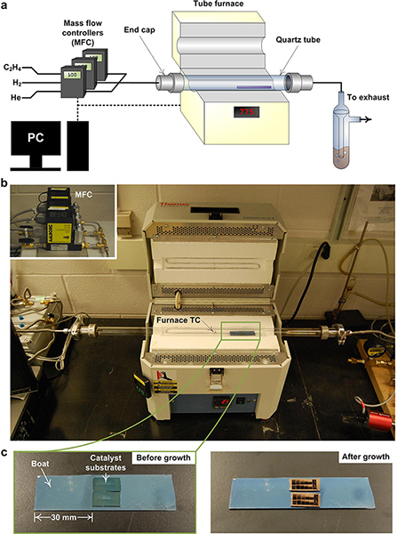
Figure 1. Tube furnace setup for growth CNT growth. (a) System schematic. (b) Tube furnace (Thermo-Fisher Minimite), with cover open to show silicon boat inside sealed quartz tube. (c) Silicon boat with samples, shown before and after growth. Click here to view larger figure.
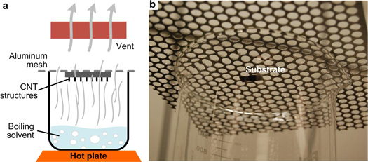
Figure 2. (a) Schematic of beaker setup for controlled condensation of solvent vapor onto CNT microstructures (image modified from De Volder et al. 6). (b) CNT sample substrate attached to aluminum mesh over boiling acetone.
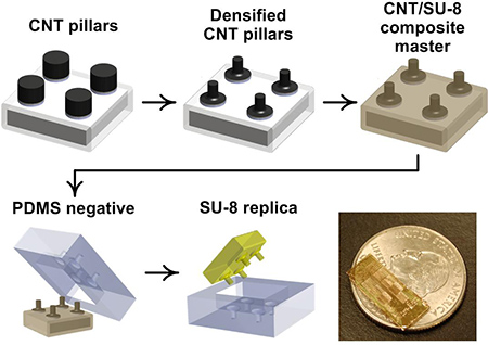
Figure 3. Process flow for replica molding of CNT microstructures, and image of representative replicated microstructure array compared to U.S. quarter dollar coin.
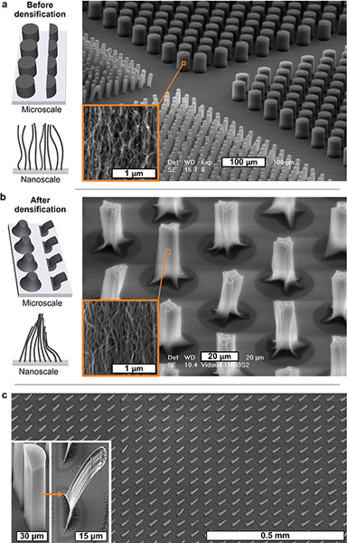
Figure 4. Exemplary CNT microstructures before and after capillary forming. Schematic and SEM images of array of cylindrical CNT pillars (a) before capillary forming, and (b) after capillary forming (image modified from De Volder et al. 6). Insets show alignment and density of CNTs. (c) Semicylindrical CNT pillars densify and tilt during capillary forming, forming inclined beams (image modified from Zhao et al. 7). Click here to view larger figure.
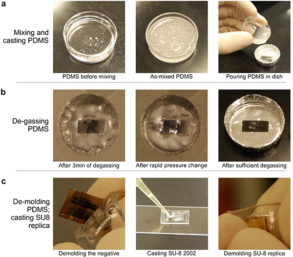
Figure 5. Key steps of CNT negative mold fabrication and replica casting. (a) Casting of PDMS negative mold. (b) Degassing of the negative mold. (c) Manual demolding of the negative, and casting of the SU-8 replica.

Figure 6. Comparison of (a) CNT/SU-8 master and (b) replica micropillar structures showing high fidelity replication of micro-scale shape and nanoscale texture (i.e., sidewalls and top surface), over a large area (image modified from Copic et al. 5). Click here to view larger figure.
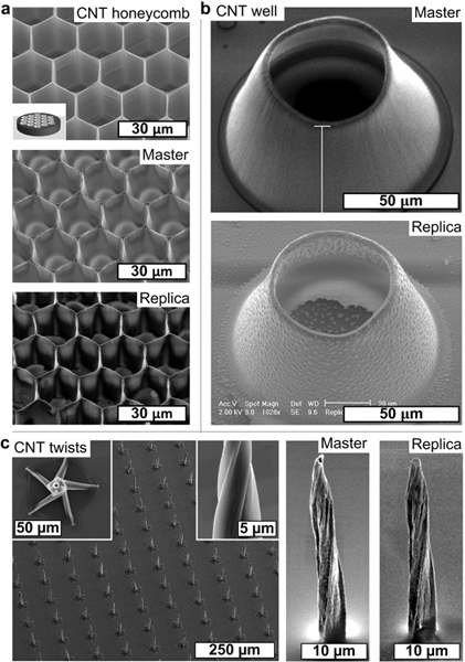
Figure 7. High-aspect-ratio (HAR) and re-entrant CNT microstructures and their polymer replicas. (a) Densified CNT honeycomb with corresponding SU8-CNT master and SU8 replica. (b) Master and replica of sloped CNT microwell (image modified from Copic et al. 5). (c) Densified twisted CNT micropillars, with master and replica of individual structure (image modified from De Volder et al. 4). The honeycombs in (a) have wall width of 400 nm and height of 20 μm. Click here to view larger figure.
Dyskusje
Lithographic patterning and preparation of the CNT catalyst substrates is straightforward and repeatable; however, achieving consistent CNT growth requires careful attention to how the height and density of CNT forests are impacted by the ambient humidity and the condition of the growth tube. In our experience, patterns larger than 1000 μm2 are less sensitive to small fluctuations in the processing conditions. Further, the density of the patterns plays affects the growth density and height8. T...
Ujawnienia
No conflicts of interest declared.
Podziękowania
This research was supported by the Nanomanufacturing program of the National Science Foundation (CMMI-0927634). Davor Copic was supported in part by the Rackham Merit Fellowship Program at the University of Michigan. Sameh Tawfick acknowledges partial support from the Rackham Predoctoral Fellowship. Michael De Volder was supported by the Belgian Fund for Scientific Research - Flanders (FWO). Microfabrication was performed at the Lurie Nanofabrication Facility (LNF), which is a member of the National Nanotechnology Infrastructure Network; and electron microscopy was performed at the Michigan Electron Microbeam Analysis Laboratory (EMAL).
Materiały
| Name | Company | Catalog Number | Comments |
| Name of the reagent | Company | Catalogue number | Comments |
| 4" diameter <100> silicon wafers coated with SiO2 (300 nm) | Silicon Quest | Custom | |
| Positive photoresist | MicroChem | SPR 220-3.0 | |
| Hexamethyldisilizane (HMDS) | MicroChem | ||
| Developer | AZ Electronic Materials USA Corp. | AZ 300 MIF | |
| Sputtering system | Kurt J. Lesker | Lab 18 | Sputtering system for catalyst deposition |
| Thermo-Fisher Minimite | Fisher Scientific | TF55030A | Tube furnace for CNT growth |
| Quartz tube | Technical Glass Products | Custom | 22 mm ID × 25 mm OD 30" length |
| Helium gas | PurityPlus | He (PrePurified 300) | |
| Hydrogen gas | PurityPlus | H2 (PrePurified 300) | UHP |
| Ethylene gas | PurityPlus | C2H4 (PrePurified 300) | UHP |
| Perforated aluminum sheet | McMaster-Carr | 9232T221 | For holding sample above densification beaker |
| UV flood lamp | Dymax | Model 2000 | |
| SU-8 2002 | MicroChem | SU-8 2002 | |
| Polydimethylsiloxane (PDMS) | Dow Corning | Sylgard 184 Silicone Elastomer Kit |
Odniesienia
- Xia, Y. N., Whitesides, G. M. Soft lithography. Annual Review of Materials Science. 28, 153-184 (1998).
- Xia, Y. Replica molding using polymeric materials: A practical step toward nanomanufacturing. Advanced Materials. 9, 147-149 (1997).
- Tasis, D., Tagmatarchis, N., Bianco, A., Prato, M. Chemistry of Carbon Nanotubes. Chemical Reviews. 106, 1105-1136 (2006).
- De Volder, M. Diverse 3D Microarchitectures Made by Capillary Forming of Carbon Nanotubes. Advanced Materials. 22, 4384-4389 (2010).
- Copic, D., Park, S. J., Tawfick, S., De Volder, M. F. L., Hart, A. J. Fabrication of high-aspect-ratio polymer microstructures and hierarchical textures using carbon nanotube composite master molds. Lab on a Chip. 11, 1831-1837 (2011).
- De Volder, M. F. L., Park, S. J., Tawfick, S. H., Vidaud, D. O., Hart, A. J. Fabrication and electrical integration of robust carbon nanotube micropillars by self-directed elastocapillary densification. Journal of Micromechanics and Microengineering. 21, 045033-04 (2011).
- Zhao, Z. Bending of nanoscale filament assemblies by elastocapillary densification. Physical Review E. 82, 041605 (2010).
- De Volder, M. F. L., Vidaud, D. O., Meshot, E. R., Tawfick, S., Hart, A. J. Self-similar organization of arrays of individual carbon nanotubes and carbon nanotube micropillars. Microelectronic Engineering. 87, 1233-1238 (2010).
- Nessim, G. D. Tuning of Vertically-Aligned Carbon Nanotube Diameter and Areal Density through Catalyst Pre-Treatment. Nano Letters. 8, 3587-3593 (2008).
- Pokroy, B., Epstein, A. K., Persson-Gulda, M. C. M., Aizenberg, J. Fabrication of Bioinspired Actuated Nanostructures with Arbitrary Geometry and Stiffness. Advanced Materials. 21, 463-469 (2009).
Przedruki i uprawnienia
Zapytaj o uprawnienia na użycie tekstu lub obrazów z tego artykułu JoVE
Zapytaj o uprawnieniaPrzeglądaj więcej artyków
This article has been published
Video Coming Soon
Copyright © 2025 MyJoVE Corporation. Wszelkie prawa zastrzeżone