
A subscription to JoVE is required to view this content. Sign in or start your free trial.
Method Article
Plasma-assisted Molecular Beam Epitaxy of N-polar InAlN-barrier High-electron-mobility Transistors
In This Article
Summary
Molecular beam epitaxy is used to grow N-polar InAlN-barrier high-electron-mobility transistors (HEMTs). Control of the wafer preparation, layer growth conditions and epitaxial structure results in smooth, compositionally homogeneous InAlN layers and HEMTs with mobility as high as 1,750 cm2/V∙sec.
Abstract
Plasma-assisted molecular beam epitaxy is well suited for the epitaxial growth of III-nitride thin films and heterostructures with smooth, abrupt interfaces required for high-quality high-electron-mobility transistors (HEMTs). A procedure is presented for the growth of N-polar InAlN HEMTs, including wafer preparation and growth of buffer layers, the InAlN barrier layer, AlN and GaN interlayers and the GaN channel. Critical issues at each step of the process are identified, such as avoiding Ga accumulation in the GaN buffer, the role of temperature on InAlN compositional homogeneity, and the use of Ga flux during the AlN interlayer and the interrupt prior to GaN channel growth. Compositionally homogeneous N-polar InAlN thin films are demonstrated with surface root-mean-squared roughness as low as 0.19 nm and InAlN-based HEMT structures are reported having mobility as high as 1,750 cm2/V∙sec for devices with a sheet charge density of 1.7 x 1013 cm-2.
Introduction
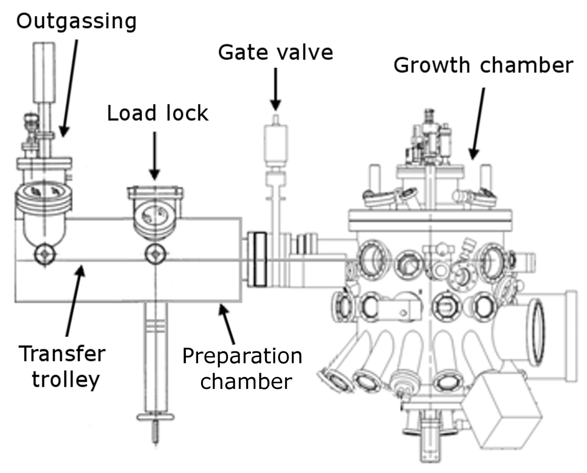
Molecular beam epitaxy (MBE) is a versatile epitaxial thin film growth technique that employs an ultra-high vacuum environment with base pressures as low as 10-11 Torr to ensure low impurity incorporation in the grown film. The composition and growth rate of the epitaxially grown layers are determined by controlling the temperature of each effusion cell, and thus the evaporated flux of the various source materials. In the case of III-nitride epitaxy, the group III-elements (In, Al, Ga) are typically provided by effusion cells while the active nitrogen (N*) flux is provided by either an N2 plasma1,2 (RF plasma-assisted MBE: PAMBE or RFMBE) or ammonia (NH3-MBE).3,4 MBE growth is characterized by lower growth temperatures and sharper interfacial abruptness than other epitaxial growth techniques, such as metalorganic chemical vapor deposition.5 A schematic is shown in Figure 1.

Figure 1: MBE system schematic. Schematic showing the load lock, transfer system, outgassing station and growth chamber. Please click here to view a larger version of this figure.
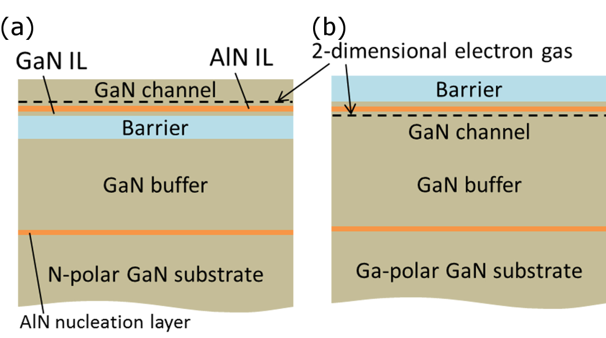
III-nitrides can be grown on substrates having a variety of crystal orientations. The most commonly used orientation is the Ga-polar c-plane, which allows the formation of a two-dimensional electron gas without doping by utilizing the difference in polarization between the barrier layer, typically AlGaN, and GaN channel. Various non-polar and semi-polar orientations of GaN have received significant attention for optoelectronics due to reduced polarization effects in the quantum wells,6,7 which also makes these orientations less desirable for HEMT applications. N-polar oriented devices are attractive for next-generation high-frequency HEMT operation due to several intrinsic advantages over conventional Ga-polar devices.8 The barrier layer in N-polar devices is grown beneath the GaN channel as shown in Figure 2, resulting in a natural back barrier that aids electrostatic control of the channel and reduces short channel effects, while allowing easier current access to the GaN channel and reducing contact resistance. The barrier can also be controlled separately from the channel, so that as the channel thickness is scaled down for high-frequency devices the barrier design can be modified to compensate for channel charge lost to Fermi level pinning effects.

Figure 2: Epitaxial layer schematic. Layer structure of (a) an N-polar HEMT and (b) a Ga-polar HEMT for comparison. Please click here to view a larger version of this figure.
HEMTs used in high-speed, high-power amplifiers are normally grown on SiC substrates to take advantage of the high thermal conductivity of SiC. Low threading dislocation density freestanding GaN substrates can be employed to improve the electron mobility,9 thus improving the high-frequency performance. Following the growth of an AlN nucleation layer, a thick GaN buffer is grown to spatially separate the impurities at the regrowth interface from the HEMT channel and improve electrical isolation. Unlike other III-V materials, GaN grown by PAMBE typically needs growth conditions with a group-III/V ratio greater than 1, i.e., metal-rich conditions,10,11 in order to achieve a smooth surface morphology. InxAl1-xN is an alternative barrier material for III-nitride HEMTs, and has received significant attention recently because it can be grown lattice matched to GaN for x ≈ 0.18 and can generate over twice the channel charge relative to AlGaN barriers due its high spontaneous polarization.12-15 Unlike AlGaN barriers, Ga will incorporate preferentially to In in InAlN layers,16 thus care must be taken to ensure the surface is free of excess Ga after the Ga-rich GaN buffer layer growth and prior to InAlN growth.
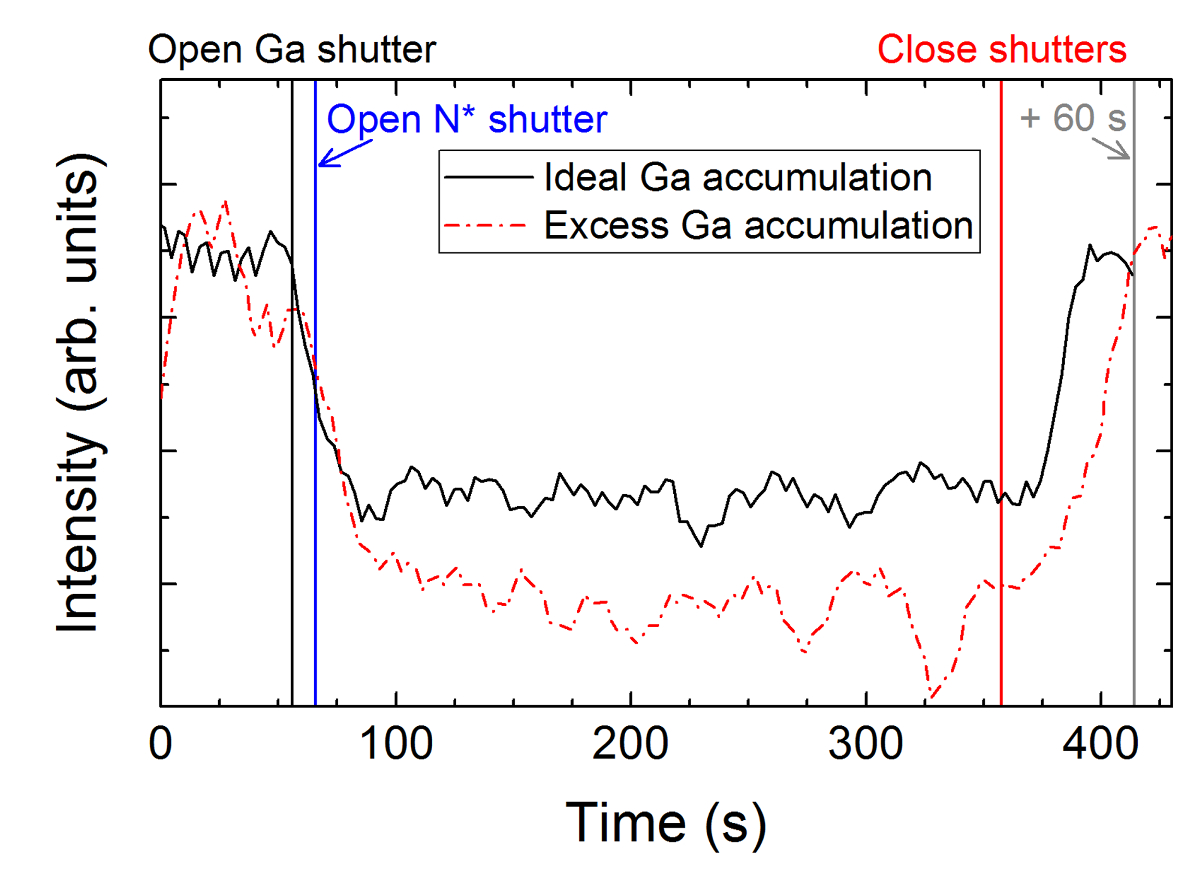
Control of Ga on the surface can be accomplished by suppling a Ga flux slightly less than the flux required for Ga-droplet formation. However, this growth window is small, and insufficient Ga surface coverage will cause the surface morphology to degrade into plateau/trench morphology while excess Ga flux will result in Ga accumulation and macroscopic droplet formation.17 Reflection high-energy electron diffraction (RHEED) intensity can be used to monitor Ga accumulation and desorption. Ga surface coverage is indicated by a reduction in RHEED intensity, and any lag between closing the Ga (and N*) shutters and the initial increase in RHEED intensity indicates accumulation of Ga, as shown in Figure 3.

Figure 3: Monitoring Ga coverage with RHEED intensity. RHEED intensity signal measured from RHEED pattern acquired under rotation using triggered acquisition. Insufficient Ga flux is indicated by an immediate increase in intensity after closing the shutters (not shown). Saturated/ideal Ga coverage is indicated by a delay between shutter closure and abrupt RHEED brightening and excess Ga coverage in seen as both a delay in initial RHEED brightening as well as a more gradual intensity increase resulting in full intensity recovery taking longer than 60 s. Please click here to view a larger version of this figure.
Achieving high quality InAlN by PAMBE is complicated by the presence of lateral composition fluctuations, resulting in a "honeycomb" microstructure consisting of Al-rich domains surrounded by In-rich boundaries.18 Elimination of this microstructure is achieved by using a substrate temperature about 50 °C above the onset of In desorption,15,19,20 or approximately 630 °C for N-polar InAlN. In this high temperature growth regime, the InxAl1-xN composition is a strong function of substrate temperature, with higher temperatures resulting in lower In incorporation. The In flux can be increased to compensate for In lost to evaporation, although in practice the maximum In flux is limited by a reduction in incorporation efficiency with increasing In flux.21 In addition to reducing the substrate temperature or increasing the In flux, increasing the growth rate can also increase the In composition due to the "In burying effect", where incoming Al atoms trap In and prevent it from evaporating.21,22 Higher growth rates can be achieved by increasing the In and Al flux proportionally. To keep the growth conditions N-rich, the N* would need to be increased as well, which can be achieved by increasing the RF plasma power, increasing the N2 flow rate, improving the plasma chamber design, or increasing the aperture plate hole density.
Additional epitaxial layers in InAlN-based HEMTs include GaN and AlN interlayers (ILs) and a GaN channel. An AlN IL inserted between the barrier and channel can increase mobility µ as well as channel sheet charge density ns. The increase in mobility is attributed to reducing electron wave function overlap with the InAlN barrier and subsequent alloy scattering.9 To ensure high-quality growth of the AlN IL, an excess of Ga flux is supplied during growth to act as a surfactant. A GaN IL can be used between the AlN IL and barrier to further improve the mobility while reducing channel charge. The GaN channel can be grown at the same temperature as the InAlN barrier, allowing continuous growth from the barrier though the ILs and channel. Improved mobility has been obtained by interrupting growth after the AlN IL and increasing the growth temperature before growing the GaN channel. In this case a protective Ga surface coverage has to be maintained during the interrupt to prevent mobility degradation.
The following protocol applies specifically to InAlN-barrier HEMTs grown on N-polar GaN substrates. It can be directly extended to growth on C-polar 4H- or 6H-SiC substrates by including a 50 nm thick N-rich AlN layer.
Protocol
1. Effusion Cell Ramp and Flux Calibration
- Confirm liquid N2 is flowing to the cryo-panels and that the growth chamber has reached base pressure.
- Ramp up the effusion cells to their beam flux measurement (BFM) temperature at a ramp rate of 1 °C/sec for Ga and In cells, and 10 °C/min for Al. Wait 1 hr for cells to thermally stabilize.
- Open the shutter of each cell for 30-60 sec, and then close the shutter for 1-2 min. Repeat three times for each cell. Discard the first beam flux ion gauge measurement and average the second two. Adjust the cell temperature to achieve the desired flux according to previous flux/temperature calibrations.
2. Substrate Preparation and Loading
- Ex situ substrate cleaning
- Load epi-ready N-polar GaN substrates directly, without any ex situ cleaning. If the wafer has been exposed to air for more than a few hours, rinse under acetone (30 sec), isopropanol (30 sec) and de-ionized (DI) water (60 sec). Rinsing is preferred to immersion when possible as it tends to leave less particles on the wafer surface.
NOTE: For Ga-polar GaN substrates a more rigorous surface clean is recommended.23
- Load epi-ready N-polar GaN substrates directly, without any ex situ cleaning. If the wafer has been exposed to air for more than a few hours, rinse under acetone (30 sec), isopropanol (30 sec) and de-ionized (DI) water (60 sec). Rinsing is preferred to immersion when possible as it tends to leave less particles on the wafer surface.
- Load wafer
- Close the load-lock isolation gate valve, and vent with N2.
- Load the wafer on the holder and return the cassette to the load lock. Turn on the load lock roughing pump and open the roughing pump valve and manifold valve.
- When the manifold pressure has dropped below 0.1 Torr, close the manifold and roughing pump valves. Turn off the roughing pump and open the load-lock turbo-pump isolation valve.
- Allow the load lock to pump down for 30-60 min. Ideally, use a load lock pressure of 10-6-10-7 Torr before transferring to the preparation chamber.
- Open the load lock into the preparation chamber, and transfer the wafer to the trolley using wobble stick. Then use the trolley to transfer the wafer to the outgassing station in the preparation chamber. Move the trolley manually along a rail using a rotary feedthrough on the preparation chamber.
- Outgas wafer
- Ramp the outgassing station heater temperature to 700 °C over 10 min.
- After 30 min, ramp the temperature back down to 100 °C. When the temperature is ≤ 250 °C, transfer the wafer back to the trolley using the wobble stick at the outgassing station.
- Load wafer into the growth chamber
- Lower the substrate manipulator to the load position, open the preparation/growth chamber gate valve and transfer the wafer holder to the manipulator.
- Raise the manipulator to growth position, near the substrate heater.
- Remove the trolley and close the gate valve.
- Open the N2 bottle valve, regulator valve and isolation needle valve. Set the mass flow controller (MFC) to 1.5 sccm (or as needed to get a chamber pressure of 3-4 x 10⁻⁵ Torr). The optimal pressure for plasma ignition is strongly system dependent. Note that the N2 must be ultra-high purity (preferably better than 6N) and an additional filter is used in line to further reduce impurities.
- With the N* and main shutters closed, turn on the plasma RF power supply and auto-matching network controller. Increase the RF power until the plasma ignites.
- Set the RF power and N2 flow to the desired process conditions, in this case 350 W and 2.0 sccm. The N* flux resulting from given plasma conditions is system dependent, but here, these conditions yield a GaN growth rate of 5.0 nm/min, or a N* flux of 1.8 nm-2sec-1. Monitor the plasma stability with a spectrometer attached to the rear window of the plasma chamber.
- In situ surface preparation: Ga deposition and desorption
- Ramp up the substrate heater to 10 °C above the desired GaN growth temperature with a ramp rate of ≤1 °C/sec. In this case, use an estimated wafer temperature of 730 °C.
- Turn on the RHEED system to watch for degradation of the wafer surface and monitor Ga coverage. Manually turn on the substrate rotation. Set up the triggered RHEED acquisition software to collect a RHEED pattern once per substrate rotation to provide a static image while the substrate is rotating during growth.
- Open the substrate shutter and Ga shutter for 1 min. Ensure the RHEED intensity decreases then reaches a plateau as Ga accumulates. Ga flux should be similar to that used for GaN growth. Here, the Ga flux is approximately, 3.7 nm-2sec-1.
- Close the shutter for 2 min and ensure the RHEED intensity increases and reaches a plateau before the end of the 2 min, indicating Ga desorption.
- Repeat Steps 2.5.2-2.5.4 three times,24 and then ramp the substrate to the GaN growth temperature.
3. HEMT Growth
- Buffer growth
- Initiate growth by opening the N* shutter for a 1 min nitridation.
- Grow a thin 1-3 nm N-rich AlN nucleation layer by opening the Al shutter. This AlN layer can help prevent threading dislocation generation,25 however, the AlN layer complicates X-ray diffraction (XRD) measurements and is not recommended for XRD-based calibration samples. Use the same Al flux as for the InAlN layer, or about 0.36 nm-2sec-1, giving a growth rate of approximately 1 nm/min.
- Close the Al and N* shutter and immediately open the Ga shutter for 10 sec to allow Ga to saturate the surface, the RHEED intensity should decrease rapidly. Open the N* shutter (with the Ga shutter still open) and grow 5 min of GaN. Use Be or C doping, especially for freestanding GaN substrates, to prevent electrical leakage currents in the buffer.
- Close the Ga and N* shutters for a 1 min growth interruption. Monitor the RHEED intensity. If the RHEED intensity immediately increases, then the Ga flux is not high enough. If the RHEED intensity increases after >30 sec or does not reach a plateau within 1 min then the Ga flux is too high. See Figure 3.
- Increase the substrate temperature by a few degrees (or reduce the Ga effusion cell temperature) to compensate for high Ga flux seen in 3.1.4. If the Ga flux was too low, decrease the substrate temperature (or increase the Ga effusion cell temperature) to compensate.
- Repeat Steps 3.1.3-3.1.5 until there is a 15-30 sec delay before the RHEED intensity increases and the RHEED intensity reaches a plateau before 1 min.
- Continue repeating Steps 3.1.4-3.1.5 until the desired GaN thickness is reached. Determine thickness by multiplying the total growth time by the calibrated growth rate. For Ga-rich growth, determine the growth rate by the N* flux, which can in turn be calculated using XRD to measure the thickness for a known growth time in a separately grown calibration sample.
- InAlN barrier growth
- Wait an additional 1 min after the final GaN growth step to ensure all Ga has evaporated.
- Quickly ramp down to the InAlN growth temperature to approximately 630 °C. Allow the substrate temperature to stabilize for about 2 min.
- Open the In, Al, and N* shutters. The RHEED intensity should decrease and reach a plateau within the first 3 min. Continued decrease of RHEED intensity may indicate accumulation of In, which is detrimental to InAlN growth. The RHEED pattern should remain streaky, indicating a smooth surface. The In and Al fluxes are about 0.31 and 0.36 nm-2sec-1, giving a group-III limited growth rate of 1.25 nm/min.
- Close the In, Al, and N* shutters after the desired barrier thickness has been reached. For N-rich growth, determine the growth rate by the total group-III flux. Measure the growth rate using XRD on a separately grown InAlN calibration sample. For a 15 nm InAlN barrier using the conditions given here, open the shutters for 12 min 30 sec.
- Interlayer and channel growth
- First open the Ga shutter for 5 sec, then open the N* shutter and grow the GaN interlayer. The substrate temperature should still be at the InAlN growth temperature.
- Open the Al shutter without closing the Ga or N* shutters to grow the AlN interlayer. The Al flux for the interlayer should be the same or slightly higher than the N* flux, ideally using a different Al effusion cell then that used for the InAlN barrier layer, to avoid having to change the cell temperature. See step 3.2.4.
- Close the N* and Al shutters but leave the Ga shutter open. Ramp the substrate temperature to the GaN channel temperature.
- After 30 sec close the Ga shutter. Wait 30 sec (or as soon as the RHEED intensity starts to increase) and re-open the Ga shutter. Continue to cycle the Ga shutter until the substrate has reached the GaN channel growth temperature. This will protect the surface while preventing excessive Ga accumulation.
- Open the Ga shutter for 5 sec, then open the N* shutter and grow the GaN channel.
- Close the Ga, N* and main shutters. Ramp the substrate temperature down to 200 °C, turn off the N* plasma and shut off the N2 gas flow.
- Ramp the cells down to their standby temperatures if finished for the day.
- Wait for the substrate temperature to decrease below 250 °C and the chamber pressure to drop below 8 x 10⁻⁷ Torr, then open the growth chamber gate valve and transfer the wafer holder back to the trolley.
- Follow the reverse of Step 2.2 to transfer the wafer back to the load lock, vent with N2 and remove the wafer. Make sure the growth chamber gate valve is closed before opening the load lock, and that the load lock turbo pump gate valve is closed before venting.
- Follow Steps 2.2.3-2.2.5 to return the cassette and load lock to high vacuum.
4. Characterization
- Characterize the material quality using optical microscopy to check for pits, cracks or Ga-droplets that may have formed during the channel growth, XRD to check the interfacial and structure quality, and AFM to check the surface morphology.20,21
- If Ga-droplets are present, immerse the wafer in concentrated HF acid for 5-10 min to remove the droplets without damaging the chemically sensitive N-polar surface.
- Measure sheet resistance using Lehighton contactless resistance measurements.
- Process the sample to allow electrical characterization, including Hall and CTLM measurements and dc and RF transistor characterization.9,26
Results
X-ray diffraction (XRD) scans of InAlN thin films shown grown on N-polar GaN substrates in Figure 4(a) are single peaked both for 50 and 200-nm-thick films. The XRD scan of the 50 nm thick InAlN film exhibits Pendellösung fringes up to 15th order, indicating very high interfacial quality. The asymmetric reciprocal space map in Figure 4(b) shows that the 200 nm thick InAlN layer has the same q‖, and thus the same in-plane l...
Discussion
Growth of a high quality GaN buffer layer is critical to achieving high electron mobility in any III-nitride HEMT. In the case of an N-polar InAlN HEMT, the buffer layer growth is complicated by the requirement that all Ga be removed from the surface prior to InAlN growth. There are a variety of techniques to accomplish this in addition to the procedure described here, such as metal-modulated epitaxy,27 using growth conditions at the edge of the intermediate Ga coverage and Ga droplet accumulation regime,...
Disclosures
The authors have nothing to disclose.
Acknowledgements
The authors thank Mr. Neil Green for assistance with sample preparation. This work was supported by the Office of Naval Research under funding from Dr. P. Maki. MTH was supported by a National Research Council Postdoctoral Fellowship.
Materials
| Name | Company | Catalog Number | Comments |
| Freestanding N-polar GaN wafer | Kyma | 10 mm x 10 mm | |
| C-polar SiC wafer | Cree | W4TRE0R-L600 | 3 inch diameter |
| Microelectronics grade acetone | Fischer Scientific | A18-4 | |
| Microelectronics grade isoproponal | J.T. Baker | 9079-05/JT9079-5 | |
| Al source material (6N5 pure) | UMC | ALR62060I | |
| Ga source material (7N pure) | UMC | GA701 | |
| In source material (7N pure) | UMC | IN750 | |
| ULSI N2 source gas (6N pure) | Matheson Tri-gas | G2659906D | |
| PRO-75 MBE system | OmicronScientia |
References
- Hughes, W. C., et al. Molecular beam epitaxy growth and properties of GaN films on GaN/SiC substrates. J. Vac. Sci. Technol., B. 13 (4), 1571-1577 (1995).
- McSkimming, B. M., Wu, F., Huault, T., Chaix, C., Speck, J. S. Plasma assisted molecular beam epitaxy of GaN with growth rates 2.6 µm/hr. J. Cryst. Growth. 386, 168-174 (2014).
- Grandjean, N., Massies, J., Leroux, M. Nitridation of sapphire. Effect on the optical properties of GaN epitaxial overlayers. Appl. Phys. Lett. 69 (14), 2071-2073 (1996).
- Corrion, A. L., Wu, F., Speck, J. S. Growth regimes during homoepitaxial growth of GaN by ammonia molecular beam epitaxy. J. Appl. Phys. 112 (5), 054903 (2012).
- Mazumder, B., et al. Atom probe analysis of AlN interlayers in AlGaN/AlN/GaN heterostructures. Appl. Phys. Lett. 102 (11), 111603 (2013).
- Feezell, D. F., Speck, J. S., DenBaars, S. P., Nakamura, S. Semipolar (2021) InGaN/GaN Light-Emitting Diodes for High-Efficiency Solid State Lighting. J. Disp. Technol. 9 (4), (2013).
- Hardy, M. T., et al. True Green Semipolar InGaN-Based Laser Diodes Beyond Critical Thickness Limits Using Limited Area Epitaxy. J. Appl. Phys. 114 (18), 183101 (2013).
- Wong, M. H., et al. N-polar GaN epitaxy and high electron mobility transistors. Semicond. Sci. Technol. 28 (7), 074009 (2013).
- Hardy, M. T., et al. Charge control in N-polar InAlN high-electron-mobility transistors grown by plasma-assisted molecular beam epitaxy. J. Vac. Sci. Technol., B. 33 (6), 061207 (2015).
- Piquette, E. C., Bridger, P. M., Beach, R. A., McGill, T. C. Effect of Buffer Layer and III/V Ratio on the Surface Morphology of GaN Grown by MBE. Symposium G '-' GaN and Related Alloys. , (1998).
- Tarsa, E. J., et al. Homoepitaxial growth of GaN under Ga-stable and N-stable conditions by plasma-assisted molecular beam epitaxy. J. Appl. Phys. 82 (11), 5472-5479 (1997).
- Kuzmik, J. Power electronics on InAlN/(In)GaN: Prospect for a record performance. IEEE Electron Device Lett. 22 (11), 510-512 (2001).
- Fernández-Garrido, S., Gačević, &. #. 3. 8. 1. ;., Calleja, E. A comprehensive diagram to grow InAlN alloys by plasma-assisted molecular beam epitaxy. Appl. Phys. Lett. 93 (19), 191907 (2008).
- Katzer, D. S., et al. Molecular beam epitaxy of InAlN∕GaN heterostructures for high electron mobility transistors. J. Vac. Sci. Technol., B. 23 (3), 1204-1208 (2005).
- Kaun, S. W., et al. GaN-based high-electron-mobility transistor structures with homogeneous lattice-matched InAlN barriers grown by plasma-assisted molecular beam epitaxy. Semicond. Sci. Technol. 29 (4), 045011 (2014).
- Hoke, W. E., Torabi, A., Mosca, J. J., Kennedy, T. D. Thermodynamic analysis of cation incorporation during molecular beam epitaxy of nitride films using metal-rich growth conditions. J. Vac. Sci. Technol., B. 25 (3), 978-982 (2007).
- Koblmüller, G., Reurings, F., Tuomisto, F., Speck, J. S. Influence of Ga/N ratio on morphology, vacancies, and electrical transport in GaN grown by molecular beam epitaxy at high temperature. Appl. Phys. Lett. 97 (19), 191915 (2010).
- Zhou, L., Smith, D. J., McCartney, M. R., Katzer, D. S., Storm, D. F. Observation of vertical honeycomb structure in InAlN∕GaN heterostructures due to lateral phase separation. Appl. Phys. Lett. 90 (8), 081917 (2007).
- Ahmadi, E., et al. Elimination of columnar microstructure in N-face InAlN, lattice-matched to GaN, grown by plasma-assisted molecular beam epitaxy in the N-rich regime. Appl. Phys. Lett. 104 (7), 072107 (2014).
- Hardy, M. T., et al. Morphological and microstructural stability of N-polar InAlN thin films grown on free-standing GaN substrates by molecular beam epitaxy. J. Vac. Sci. Technol., A. 34 (2), 021512 (2016).
- Hardy, M. T., et al. Indium incorporation dynamics in N-polar InAlN thin films grown by plasma-assisted molecular beam epitaxy on freestanding GaN substrates. J. Cryst. Growth. 245, (2015).
- Leszczynski, M., et al. Indium incorporation into InGaN and InAlN layers grown by metalorganic vapor phase epitaxy. J. Cryst. Growth. 318 (1), 496-499 (2011).
- Storm, D. F., et al. Ultrathin-barrier AlN/GaN heterostructures grown by rf plasma-assisted molecular beam epitaxy on freestanding GaN substrates. J. Cryst. Growth. 380, 14-17 (2013).
- Storm, D. F., Katzer, D. S., Meyer, D. J., Binari, S. C. Oxygen incorporation in homoepitaxial N-polar GaN grown by radio frequency-plasma assisted molecular beam epitaxy: Mitigation and modeling. J. Appl. Phys. 112 (1), 013507 (2012).
- Storm, D. F., et al. Effect of interfacial oxygen on the microstructure of MBE-grown homoepitaxial N-polar. J. Cryst. Growth. 409, 14 (2014).
- Meyer, D. J., et al. High Electron Velocity Submicrometer AlN/GaN MOS-HEMTs on Freestanding GaN Substrates. IEEE Electron Device Lett. 34, 199 (2013).
- Moseley, M., Billingsley, D., Henderson, W., Trybus, E., Doolittle, W. A. Transient atomic behavior and surface kinetics of GaN. J. Appl. Phys. 106 (1), 014905 (2009).
- Koblmüller, G., et al. Ga Adlayer Governed Surface Defect Evolution of (0001)GaN Films Grown by Plasma-Assisted Molecular Beam Epitaxy. Jpn. J. Appl. Phys. 44 (28), L906-L908 (2005).
- Poblenz, C., Waltereit, P., Speck, J. S. Uniformity and control of surface morphology during growth of GaN by molecular beam epitaxy. J. Vac. Sci. Technol., B. 23 (4), 1379-1385 (2005).
Reprints and Permissions
Request permission to reuse the text or figures of this JoVE article
Request PermissionThis article has been published
Video Coming Soon
Copyright © 2025 MyJoVE Corporation. All rights reserved