
Method Article
Preparation of Graphene-Supported Microwell Liquid Cells for In Situ Transmission Electron Microscopy
* These authors contributed equally
In This Article
Summary
A protocol for preparation of graphene-supported microwell liquid cells for in situ electron microscopy of gold nanocrystals from HAuCl4 precursor solution is presented. Furthermore, an analysis routine is presented to quantify observed etching and growth dynamics.
Abstract
The fabrication and preparation of graphene-supported microwell liquid cells (GSMLCs) for in situ electron microscopy is presented in a stepwise protocol. The versatility of the GSMLCs is demonstrated in the context of a study about etching and growth dynamics of gold nanostructures from a HAuCl4 precursor solution. GSMLCs combine the advantages of conventional silicon- and graphene-based liquid cells by offering reproducible well depths together with facile cell manufacturing and handling of the specimen under investigation. The GSMLCs are fabricated on a single silicon substrate which drastically reduces the complexity of the manufacturing process compared to two-wafer-based liquid cell designs. Here, no bonding or alignment process steps are required. Furthermore, the enclosed liquid volume can be tailored to the respective experimental requirements by simply adjusting the thickness of a silicon nitride layer. This enables a significant reduction of window bulging in the electron microscope vacuum. Finally, a state-of-the-art quantitative evaluation of single particle tracking and dendrite formation in liquid cell experiments using only open source software is presented.
Introduction
Modern materials science, chemistry and cell biology require a deep understanding of underlying dynamic processes and effects at the sub-micron scale. Despite the power of advanced optical microscopy techniques such as stimulated-emission-depletion fluorescence microscopy1, direct imaging techniques to access detailed morphologies require electron microscopy. In particular, in situ (scanning) transmission electron microscopy (S)TEM has been shown to illuminate valuable insights into process dynamics by encapsulating liquids in dedicated, vacuum-tight cells2. Various experiments such as quantitative investigations of nanostructure formation kinetics and thermodynamics3,4,5,6, imaging of biological specimens7,8,9,10 and studies of energy storage-related mechanisms11,12 along with comprehensive studies of corrosion process dynamics13 or nanobubble physics14,15,16 have unraveled many phenomena using (S)TEM that were not accessible using standard microscopy techniques.
During the last decade, two major approaches to realize in situ liquid cell TEM (LCTEM) have been established. In the first approach, the liquid is encapsulated in a cavity between two Si3N4 membranes produced via Si process technology17, whereas in the second, small liquid pockets are formed between two graphene or graphene oxide sheets10,18. The handling of both silicon-based liquid cells (SiLCs) and graphene-based liquid cells (GLCs) has been demonstrated19,20,21. Although both approaches have undergone significant improvements22,23,24,25, they still lack in the combination of the respective advantages. In general, a tradeoff exists between encapsulating the sample in often undefined graphene pockets with a small liquid volume that enables high-resolution imaging18, and well defined cell volumes resulting in thicker membranes and liquid layers, which provide an environment closer to the natural situation in bulk liquid26 at the expense of resolution2. Furthermore, some experiments depend on a liquid flow26,27 which has only been realized in SiLC architectures and requires a dedicated TEM holder28.
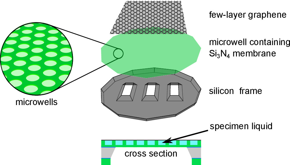
Here, we present the fabrication and handling of a liquid cell approach for high-performance in situ LCTEM via static graphene-supported microwell liquid cells (GSMLCs) for TEM analyses. A sketch of the GSMLC is presented in Figure 1. GSMLCs have proven to be capable of enabling in situ high-resolution transmission electron microscopy (HRTEM) results6 and are also feasible for in situ scanning electron microscopy29. Their Si technology-based frame allows for mass production of reproducibly shaped cells with tailored liquid thickness and extra-thin membranes from a single wafer. The graphene membrane covering these cells also mitigates electron beam-induced perturbations8,30,31 since the electron beam passes through the top graphene membrane first. The flat topography of the cells allow for complementary analysis methods such as energy-dispersive X-ray spectroscopy (EDXS)6 without any shadowing effects arising from the liquid cell itself, enabling a variety of high-quality in situ liquid cell electron microscopy experiments.
Protocol
1. Fabrication of microwell-based liquid cell templates
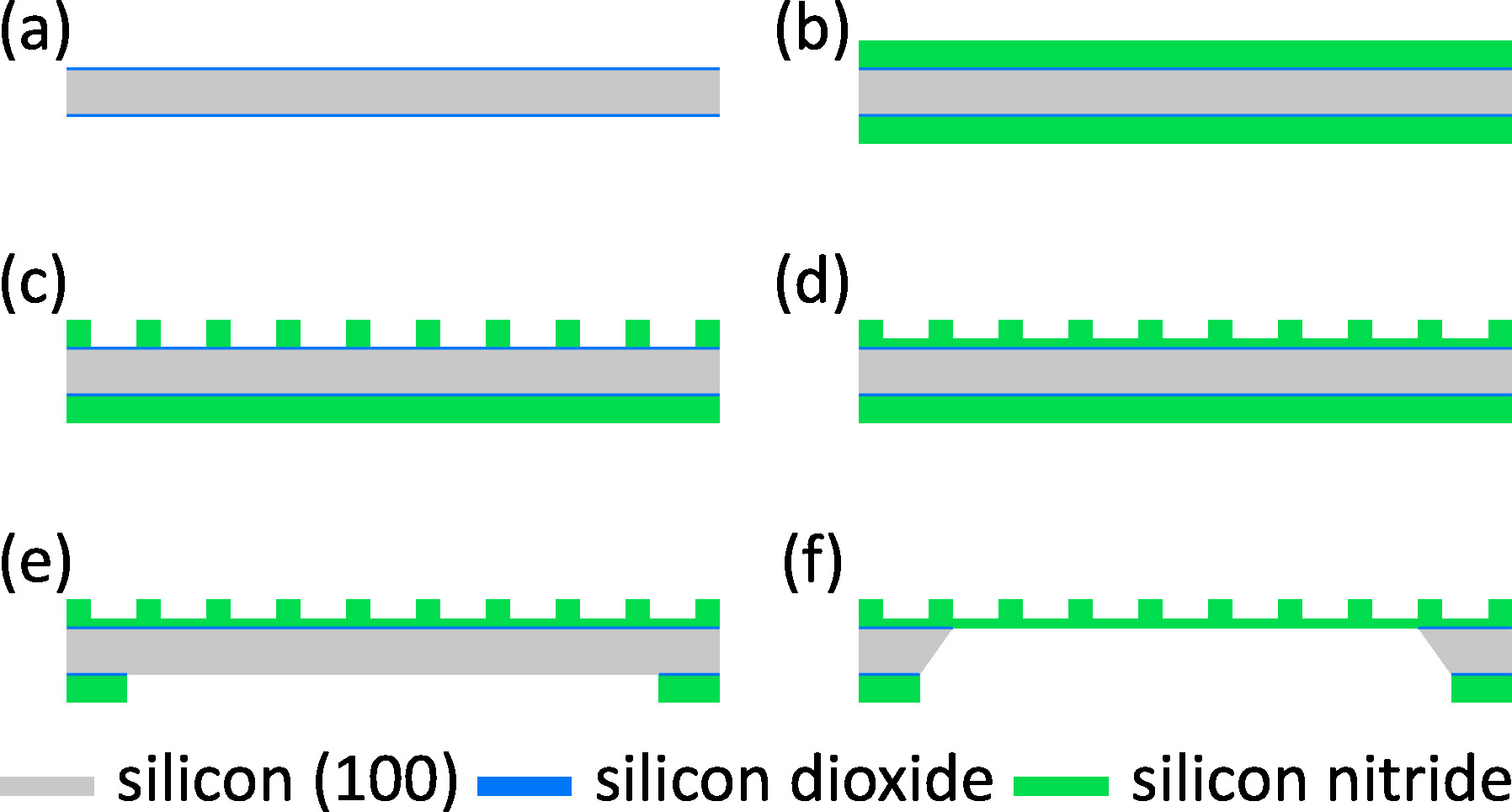
- Remove organic residues and native oxide layers from a 175 µm thick, single crystalline, boron-doped (1 – 30) Ωcm, 100 mm diameter (100) silicon wafer. Apply an oxidation step with H2O2 and TMAH, followed by a HF dip in 1 – 5% HF solution.
- Thermally oxidize the wafer in a dry oxygen atmosphere at 800 °C to grow an oxide layer with a thickness of 11 nm (Figure 2a). 3% Dichlorethene (DCE) is used to bind metallic contamination.
- Deposit a stoichiometric Si3N4 layer via low-pressure chemical vapor deposition (LPCVD). The Si3N4 layer thickness defines the well depth. Choose a value suited for the planned experiment (e.g., 500 nm) (Figure 2b).
- Define the lateral well geometry by structuring the front side via photolithography and reactive ion etching (RIE) (Figure 2c). Suitable dimensions are for example circular structures with 2.5 µm radius arranged in hexagonal arrays. Choose the well distance carefully (for example, 5 µm), to avoid instabilities in the structure.
- Deposit another 20 nm of stoichiometric Si3N4 by LPCVD, which forms the bottom membrane of the liquid cell (Figure 2d). Follow the procedure described above (see step 1.3).
- Use a second photolithography/RIE step to structure the backside which later defines the geometrical dimensions of the LC frame and its TEM windows (Figure 2e) (Frame diameter: 3 mm).
- Via bulk-micromachining in 20% KOH at 60 °C, remove the Si in the predefined area and create a free-standing Si3N4 membrane (Figure 2f).
- Remove residual metal ions in a final cleaning step with 10% HCl solution and deionized (DI) water.
2. Transfer of graphene onto TEM grids
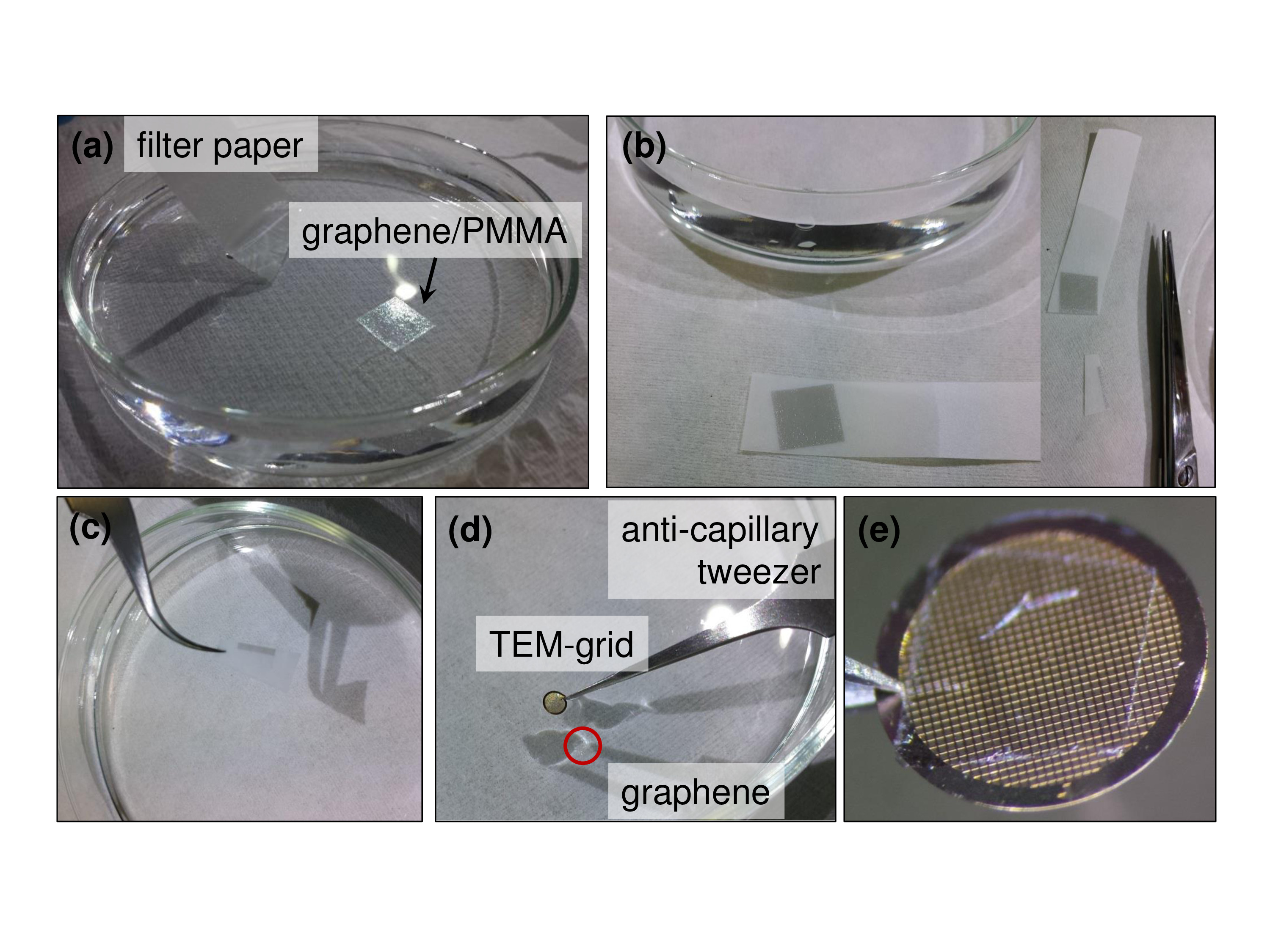
- Wet the tissue on which the commercially acquired few-layer (6 – 8) CVD-graphene on PMMA is placed. Immerse the PMMA-coated graphene in a Petri dish filled with DI water (Figure 3a).
NOTE: The number of layers of graphene can be determined using feasible techniques32,33. - Place the graphene layer on a filter paper and cut it into pieces suitable to cover all fabricated wells (e.g., 4 mm²) (Figure 3b).
- Re-immerse the cut pieces into the Petri dish (Figure 3c).
- Use a TEM grid coated with a support layer of holey carbon to fish the produced pieces out of the DI water. To do so, carefully dive the grid into the water and catch the graphene floating on the surface. Hold the grid with anti-capillary tweezers (Figure 3d,e).
NOTE: Take care that the graphene site of the graphene-PMMA stack stays on top during the whole procedure. Otherwise, the subsequent PMMA-removal will lift-off the graphene layer. - Let the sheets dry for a few hours.
- Remove the PMMA protection layer in an acetone bath for 30 min and consecutively add further cleaning steps by immersing in ethanol and DI water without drying the sample in between. Use a flat vessel (e.g., a Petri dish) to simplify the specimen transfer afterwards.
- Dry the sample afterwards for 30 min at ambient conditions.
3. Specimen preparation
- Prepare the specimen for incorporation in the GSMLC. To do so, prepare a 1 mM stock solution by solving 196.915 mg of HAuCl4·3H2O crystals in 0.5 L of DI water.
- Take the desired amount of specimen from the stock solution. Here, 0.5 µL is applied. This can be done by using a syringe or an Eppendorf pipette.
4. GSMLC loading
- Rinse the fabricated liquid cell template with acetone and ethanol.
- Apply an ambient O2/N2 (20%/80%) plasma for 5 min to enhance the wettability of the membrane.
- Dispense 0.5 µL of specimen solution on the template or the graphene layer. Ensure a smooth working procedure to minimize changes in concentration due to evaporation.
- Place the TEM grid onto the micro-patterned Si3N4 layer with the graphene facing the template. Press the graphene-coated TEM grid onto the template. Be careful not to destroy the bottom Si3N4 membrane.
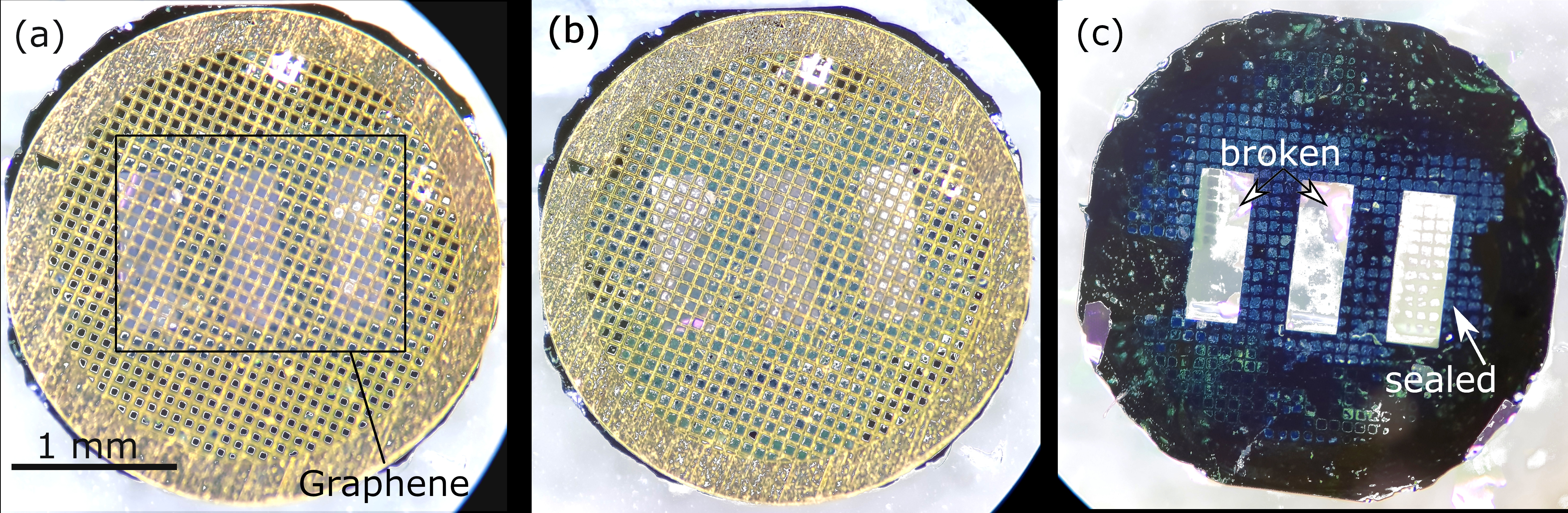
- Remove excess solution with a tissue to accelerate the cell drying and thus mitigate concentration changes (Figure 4a). After approx. 2 – 3 min, the graphene-Si3N4 van-der-Waals interaction sufficiently seal the liquid cell (Figure 4b). Alternatively, leave the cell to dry out completely without removing the excess solution. The latter offers a higher success rate in the cell processing. However, evaporation-based concentration changes in the specimen solution are expected to be more severe when using this approach.
NOTE: The successful drying process can be verified with a contrast change in the periphery (compare Figure 4a,b). - Carefully remove the TEM grid with a tweezer by pushing a tweezer tip between the grid and the GSMLC frame.
NOTE: Rash movements might break the underlying membrane. To reduce shear force damage, start from the grid site parallel to the smaller window edge. - Check, whether at least one membrane of the GSMLC is still intact via optical microscopy (Figure 4c). If all membranes were broken, LCTEM would be impossible.
5. TEM Imaging and video analysis
- Load the sample to a (S)TEM directly after preparation using a standard TEM holder.
NOTE: As it is reported for GLCs19, GSMLCs can dry out over time. Therefore, the time between loading and imaging should be minimized. - Image the sample with a suitable imaging technique, depending on both the sample and microscope. Here, a (S)TEM device operated at an acceleration voltage of 300 kV is utilized. Use a low dose to minimize beam-induced artifacts and a short exposure time to avoid movement-related blurring34. In case of long-term experiments, block the beam to reduce radiation damage.
NOTE: Due to a better temporal resolution, TEM is to be preferred over STEM for kinetic analyses34 and reduced ion reduction35. STEM, however, is preferred for investigation into thick liquid layers and high-Z elements due to its higher spatial resolution in thick specimens34,35. - Image segmentation method
- Use a suitable image processing platform to extract features of interest. For particle tracking and analysis, use the open source ImageJ-distribution FIJI36.
- Utilize the Analyze Particles function to gain precise information (projected area, barycenter) of every particle in each frame.
NOTE: This function requires binary images. - Connect the particles between the frames with the help of the plugin TrackMate37. By default, TrackMate is searching for bright particles on a dark background, so invert the images (in the case of BF-TEM) before starting TrackMate.
- Combine the results of TrackMate and Analyze Particles with a suitable script utilizing the Python-based open source ecosystem SciPy38,39.
- Use FIJI to extract the precise contours of more complex structures such as dendrites. Here, Analyze Particles can be applied, as well (see inset of Figure 6a).
NOTE: It might be feasible to analyze features of interest manually.
Results
After loading of the cell, a successful graphene transfer is indicated by a differently shaded appearance on the wells under an optical microscope. This is visible, for example, in the right membrane of Figure 3c. As mentioned, it is crucial to carefully remove the TEM-grid in order to not break the thin Si3N4 layer. In case of a broken membrane, lucent and curved residuals are clearly visible in the optical microscope, as shown in the left two membranes of Figure 3c. Due to the multiple viewing areas in the utilized GSMLC design, the cell can be used as long as at least one membrane is intact. Broken membranes can be used for TEM alignment without exposing the specimen to the electron beam.
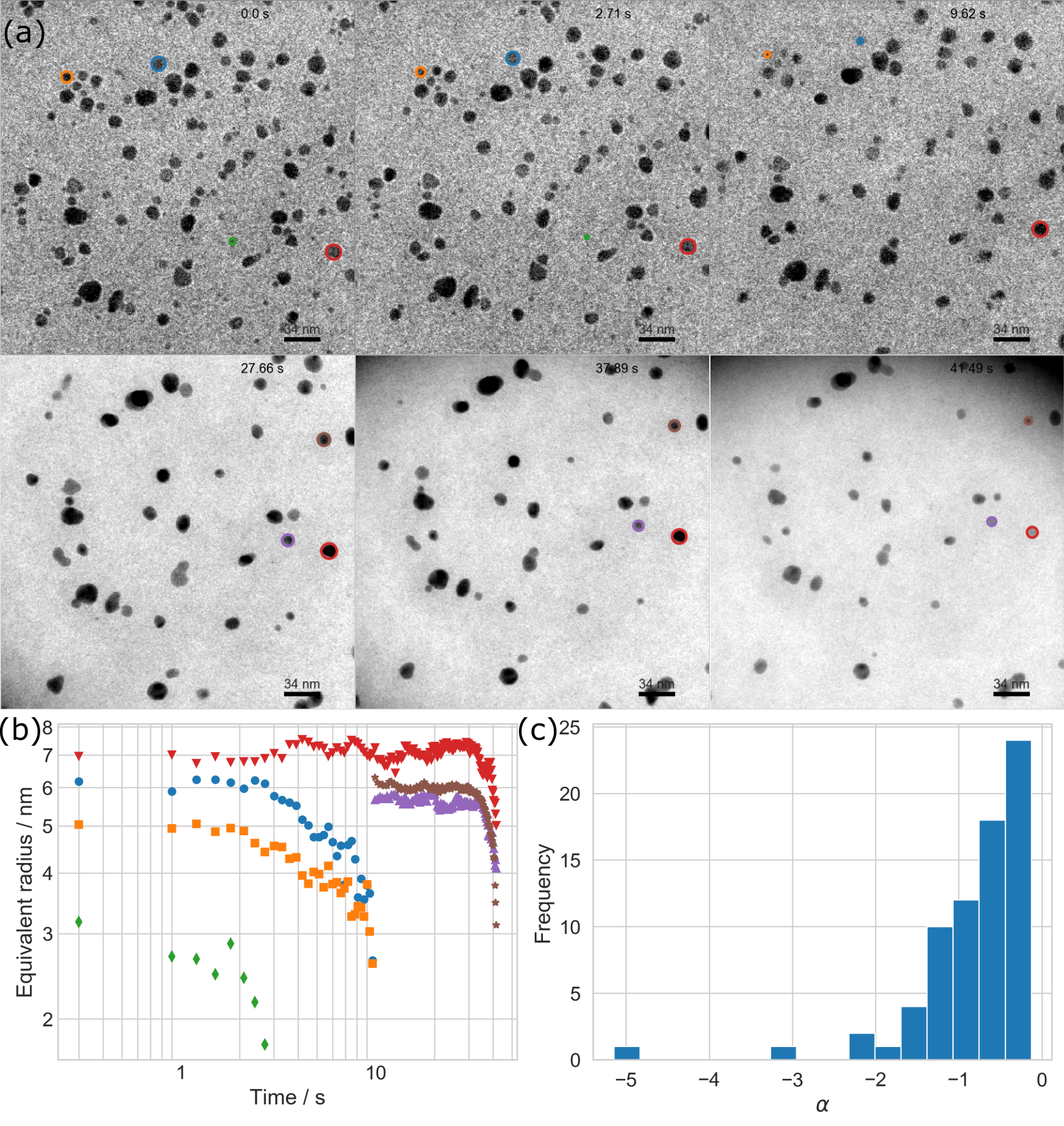
A successful encapsulation of the specimen solution can be verified during electron microscopy. Figure 5 presents individual micrographs of Supplementary Video 1, where the dissolution of an ensemble of nanoparticles and the growth of a dendritic structure is statistically evaluated in a GSMLC. Besides the drift-induced movement of the image, minor individual orthogonal particle movements are visible, indicating that particles in solution are present. Furthermore, the prevalence of particle dissolution proves that a wet-chemical reaction is present which would not be possible without a successful liquid enclosing. Other typical indications for enclosed liquids are beam-induced bubble formation19 or particle motion. The presence of Au particles in graphene-featured cells alone does not conclusively indicate a liquid environment, since the particles could also stem from the graphene-induced reduction of HAuCl440. A quantification of the oxygen peaks of the enclosed liquid via electron energy loss spectroscopy (EELS) can also be performed to verify a liquid environment41.
In order to gain insights into particle growth and dissolution kinetics, it is important to investigate each particle individually rather than to analyze the development of average parameters42. It is also crucial to exclude particles at the frame edges that are only partially captured by the camera because drift effect-related position changes of such particles might be mistaken as growth or dissolution processes. Etching is believed to be caused by oxidative species generated by electron beam-induced radiolysis43. In order to yield sufficient statistics, computational single particle tracking is required. By estimating the growth exponent α of the equivalent radius variation of individual particles over time, information of the underlying reaction kinetics can be obtained. To do so, it is possible to introduce an equivalent radius based on the projected particle area, even if not all particles are completely spherical6,44. Figure 5b shows the tracking of equivalent radii over time for six representative particles which are highlighted in Figure 5a. Figure 5c shows the distribution of α based on 73 dissolving particles from the present study. Only particles where an allometric model explains the radius decline to at least 50% (adjusted coefficient of determination) are regarded.
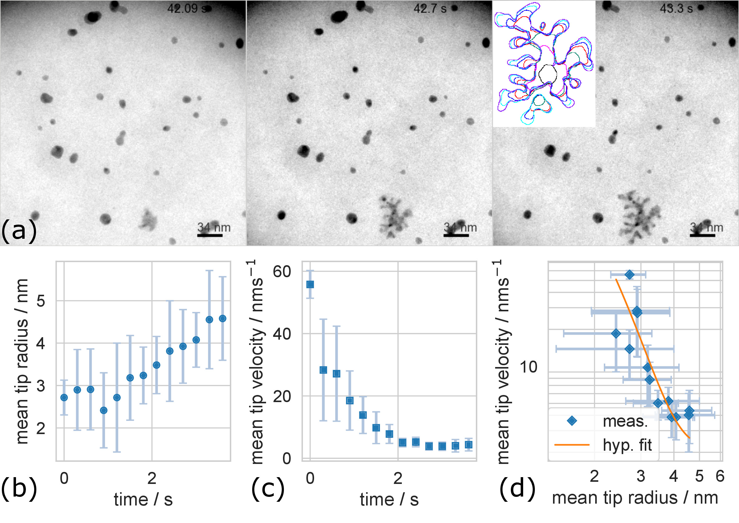
Furthermore, a dendrite structure emerges rapidly after about 42 s in the same well depicted in Figure 6a. Dendrite formation is another typical, well documented process in liquid cells45,46. To quantify dendrite growth, the structural outlines (see inset in Figure 6a) are analyzed. The evolution of tip radius and velocity over time (see Figure 6b,c) reveals the expected hyperbolic relationship47 (Figure 6d). Dendrite growth is caused by local supersaturation of Au-ions due to the aforementioned particle etching. In Figure 5a, it is clearly visible that particles are still dissolving whilst the oversaturated system relaxes into dendrite growth. This may be caused by local concentration variations in both the Au-ions and the oxidative species as a result of the high viscosity of the liquid in the GSMLC which has been observed before6. A detailed discussion of this phenomenon, however, is beyond the scope of this work.

Figure 1: Sketch of a GSMLC: Schematics of the structure of a graphene-supported microwell liquid cell. Reprinted from https://pubs.acs.org/doi/abs/10.1021/acs.nanolett.8b03388 6. Further permissions are to be directed to the American Chemical Society (ACS). Please click here to view a larger version of this figure.

Figure 2: Fabrication of GSMLC-frames. The fabrication process of GSMLC-frames is schematically sketched. (a) Oxidation of Si wafer after cleaning. (b) LPCVD of Si3N4. (c) Front side Si3N4 patterning by photolithography and RIE to define the cell volume. (d) Deposition of Si3N4 to form the bottom cell window. (e) Back-side lithography and RIE. (f) Bulk micromachining with KOH to create a freestanding Si3N4 membrane containing microwells. Please click here to view a larger version of this figure.

Figure 3: Transfer of few-layer CVD-graphene with PMMA protection layer onto a TEM-grid. The transfer of few-layer CVD-graphene on PMMA onto the top of a holey carbon-coated TEM-grid is displayed. (a) Immersion of the few-layer CVD graphene on PMMA in a Petri dish filled with DI water. (b) Transferred graphene/PMMA stack on a filter paper is cut into pieces suitable to cover the GSMLC-frames. (c) Re-immersion of a cut graphene/PMMA piece. (d) Transfer of the graphene/PMMA layer onto a holey carbon-coated TEM grid (e) Graphene/PMMA stack after a successful transfer. Please click here to view a larger version of this figure.

Figure 4: Removal of the top TEM grid. The drying process of a loaded GSMLC is documented with the help of an optical microscope. (a) A graphene-coated TEM grid is placed on top of the GSMLC directly after loading. The graphene layer is visible as turquoise rectangle covering all three viewing areas. Its outlines are roughly sketched by the black rectangle. (b) An almost completely adhered membrane is visible by the contrast change between the wet (dark, compare with (a)) and the adhered area (turquoise) after approximately two minutes. (c) A GSMLC after the lift-off of the TEM grid is shown, revealing two broken membranes (left and middle), and one membrane with successfully loaded and sealed microwells (right). Please click here to view a larger version of this figure.

Figure 5: Representative development of nanoparticle radii. The radius development of 183 individual particles has been tracked. (a) Image sequence taken from Supplementary Video 1. Six representative particles are highlighted. The colored circles correspond to the obtained equivalent radius. (b) Logarithmic plot of the particle radii. (c) The histogram of 73 particles where a negative allometric exponent α has been determined using an automated routine. Please click here to view a larger version of this figure.

Figure 6: Dendrite dynamics: The tip radius of five dendrite branches is analyzed. Error bars account for the respective standard deviation. (a) Image sequence taken from Supplementary Video 1 showing the emerging dendrite, which is visible after about 42 s. The inset in the right image shows the evolving dendrite contours. Here, the pink outlines correspond to 42.09 s, red to 42.7 s, and purple to 43.3 s. (b) Development of the (averaged) tip radius over time. (c) The mean tip velocity plotted over time. (d) The averaged tip radius logarithmically plotted against the averaged tip velocity, revealing a hyperbolic dependency (orange curve). Please click here to view a larger version of this figure.

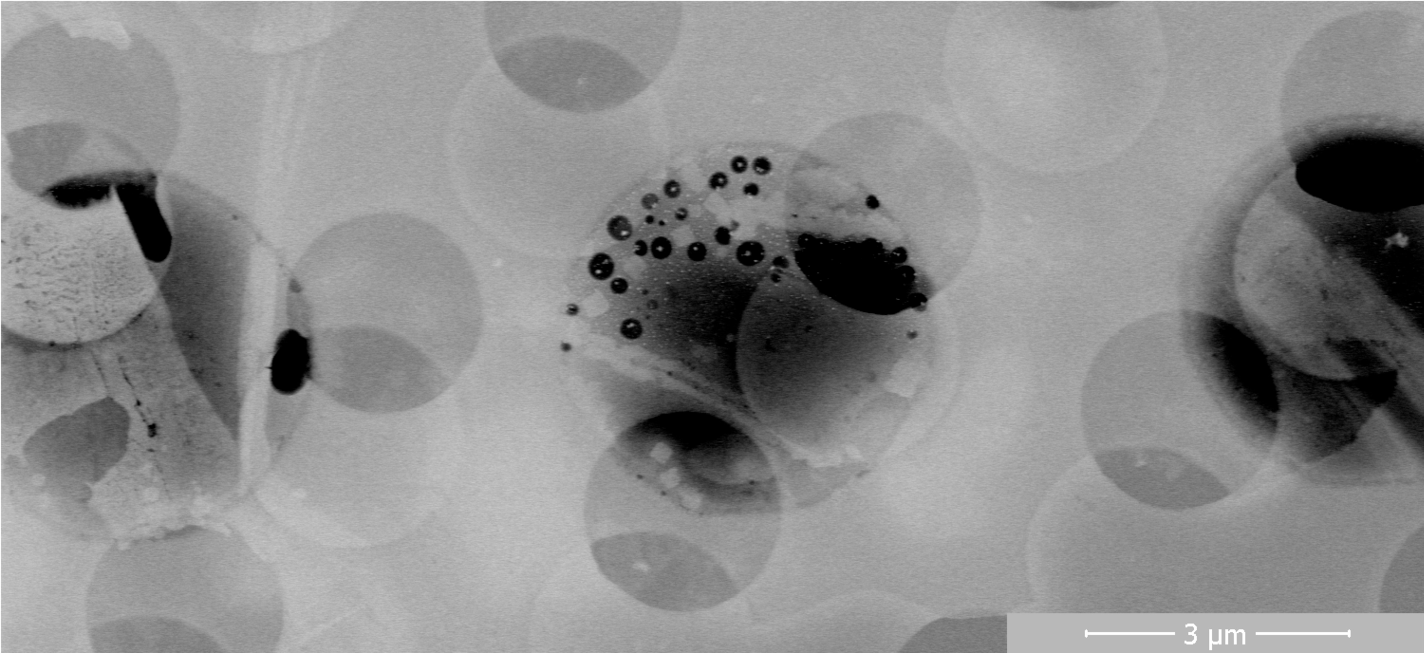
Figure 7: SEM Image of a loaded GSMLC: A representative SEM image acquired in HAADF STEM mode in an SEM of a loaded GSMLC at low acceleration voltage (29 kV) is displayed. Besides the prominent 5 µm wide microwells, two partially overlapping circular holey carbon grids (2 µm diameter) stemming from the graphene transfer elucidated above is visible. The first carbon grid stems from an unsuccessful graphene transfer. It is clearly visible that the membrane shading stays mostly constant over the well region, but slightly darkens towards the well center. This accounts for weak, negative bulging. Please click here to view a larger version of this figure.
Supplementary Video 1: In situ video showing representative results of a liquid cell bright field TEM study of etching of Au nanoparticles and subsequent growth of a dendrite structure caused by supersaturation of the surrounding specimen solution. Please click here to download this file.
Discussion
In contrast to commercially available liquid cells, custom-made GSMLCs have the advantage that they can be designed to fit into readily available TEM holders and do not require an expensive, dedicated liquid cell TEM holder.
The GSMLC architecture demonstrated here combines aspects of SiLCs and GLCs that could potentially lead to unique advantages. On the one hand, SiLCs allow for a precise determination of cell position and shape, but require relatively thick Si3N4 membranes to reduce bulging effects while ultimately reducing the achievable resolution. GLCs, on the other hand, exhibit exceptionally thin membrane walls consisting of graphene, yet suffer from random pocket sizes and positions. By combining these two membrane approaches via GSMLCs, the resolution limitation caused by the cell boundaries35 can be bypassed. As the well structure is fabricated directly into the Si3N4 layer, the actual Si3N4 membrane can be constructed even smaller than in SiLCs, simplifying HRTEM analyses which has already been demonstrated in GSMLCs6. Still, it should be noted that HRTEM in general is possible with SiLCs as well48. Moreover, large viewing areas can be realized without severe window bulging due to the small membrane areas of the individual specimen chambers. Thereby, bulging-related thickness increase35 can be ruled out to a large extent, as shown by Dukes et al.49. This is demonstrated in Figure 7, where a representative high-angle annular dark field (HAADF) STEM image of al loaded GSMLC is displayed. This image was acquired using a Dual-beam system. Since the image brightness acquired in this setup is directly related to the specimen thickness, it is clearly visible that the sealed microwells exhibit only small negative bulging. Kelly et al.24 have demonstrated that the negative bulging and partial well drying visible in Figure 7 depends on the well diameter. Reducing the well diameter is therefore a feasible approach to homogenize the liquid thickness even further.
Due to the equilibrium pocket shape of GLCs, the liquid thickness is also strongly site-dependent35. SiLCs follow the design of two membranes stemming from different Si wafers. By replacing the top Si3N4 membrane with graphene, liquid-cell fabrication is simplified. This means that possible delamination of two bonded Si-wafers during the subsequent wet etching steps can be avoided and the alignment of two wafer pieces during the cell loading is omitted. The flat surface on one side of this cell architecture enables complementary in situ analysis methods such as EDXS analysis of the specimen6, which is restricted in conventional SiLC architectures by shadowing effects at steep Si edges50.
Sealing prepatterned microwells with graphene on both the bottom and top well site has been demonstrated before24,25. Applying two graphene membranes may enhance the achievable resolution. A twofold graphene transfer, however, would complicate the preparation process further; especially since this has proven to be the most sensitive preparation step (see below). Furthermore, the above discussed membrane bulging is expected to be even more critical in case of two graphene membranes, because graphene is much more flexible than a Si3N4 layer. In those architectures, the microwells were constructed using sequential focused ion beam (FIB) milling. While this approach has proven to yield high-quality results, FIB milling is complicated and expensive cell production technique. Utilizing massively parallel single-shot patterning techniques that are already standard in today’s semiconductor industry such as nanoimprint- or photolithography, however, has the major advantage of being fast, cheap and scalable for mass production.
It should be noted that the approach presented here does not allow for liquid flow operation, which is achievable by other designs28. Since the loading and liquid volume are comparable for GSMLCs and GLCs, a contamination of high vacuum due to rupture of the membrane can be avoided19. This eliminates the need for a cumbersome seal check. Though the advantages of SiLCs and GLCs have been combined, the disadvantages of both approaches are still present in GSMLCs. The fabrication of the cells requires a clean room infrastructure for silicon technology, which is not necessarily present in TEM laboratories. In addition, the liquid loading is not trivial. It requires a dedicated training, similar to graphene cells. This, however, is also true for commercially available systems. Here, the most sensitive preparation step is the TEM-grid removal after the graphene transfer because rash movements or jittering is likely to break the Si3N4 layer. The redundant membrane windows, however, enhance the chances of preserving at least one membrane area. As a consequence, the yield (amount of operable GSMLC chips) achieved by a trained experimenter is three out of four6, and thus exceeds the one achieved with graphene-based cells (one to two out of four)19.
As with GLCs, the liquid encapsulation in GSMLCs is based on van-der-Waals interactions18. Consequently, interface contamination could lower the success rate in processing of GSMLCs19. Furthermore, depending on the Hamaker constant of the to-be-encapsulated liquid phase, the wetting characteristics during the loading procedure (and thus the achievable yield) may differ51 and therefore the preparation can be complicated. Our experience shows that this is the case if, for example, amphiphilic species are present.
The GSMLC architecture enables flexible configuration of well-depths, allowing for adaptation to various experimental prerequisites. Moreover, the architecture is suitable for electron tomography investigations over a broad tilt-angle range of ±75 °, which would also allow for in situ electron tomography52. Therefore, in situ and post mortem tomography of specimen in liquid could also be established with GSMLCs.
Disclosures
We have nothing to disclose.
Acknowledgements
We thank Tilo Schmutzler for the preparation of the HAuCl4 solution. Furthermore, we thank R. Christian Martens for proof reading. Financial support by the German Research Foundation (DFG) via the Research Training Group GRK 1896 “In situ microscopy with electrons, X-rays and scanning probes” and through the Cluster of Excellence EXC 315/2 EAM “Engineering of Advanced Materials” is gratefully acknowledged.
Materials
| Name | Company | Catalog Number | Comments |
| Acetone | VWR Chemicals | 50488858 | VLSI |
| Deionized water | own production | ||
| Dumont Anti-Capillary tweezers | Carl Roth GmbH + Co. KG | LH72.1 | 0203-N5AC-PO Dumoxel alloyed |
| Ethanol | VWR Chemicals | 85651.360 | VLSI |
| FIJI Is Just ImageJ | FIJI.sc | Version 1.51 | |
| Gold Quantifoil, Amorphous Carbon TEM Grids | Plano GmbH | S173-8 | R 2/2 Au 300 mesh |
| HAuCl4 · 3 H2O crystal | Alfa Aesar | 36400.06 | 5 g |
| Jupyter Notebook | Project Jupyter | Version 5.7.2 | |
| Matplotlib-Package | John Hunter, Darren Dale, Eric Firing, Michael Droettboom and the Matplotlib development team | Version 3.0.2 | |
| NumPy-Package | NumPy developers | Version 1.15.4 | |
| Pandas-Package | AQR Capital Management, LLC, Lambda Foundry, Inc. and PyData Development Team | Version 0.23.4 | |
| Python | Python Software Foundation | Version 3.7 | |
| Scipy-Package | SciPy developers | Version 1.1.0 | |
| Seaborn-Package | Michael Waskom | Version 0.9.0 | |
| Si wafer | Siegert Wafer GmbH | Thin silicon (100) wafer 175 +/-5 µm, 4", p-type, boron doped (1-30 Ohm cm), double-sided polished | |
| single tilt TEM holder | Philips | Ensure that cell fits | |
| Transmission Electron Microscope | Philips | CM 30 (S)TEM | 300 kV |
| Trivial Transfer Graphene | ACS Material | TTG60011 | PMMA-covered, 6 -- 8 MLs |
References
- Hell, S. W., Wichmann, J. Breaking the diffraction resolution limit by stimulated emission: stimulated-emission-depletion fluorescence microscopy. Optics Letters. 19 (11), 780 (1994).
- Ross, F. M. . Liquid Cell Electron Microscopy. , (2016).
- Alloyeau, D., et al. Unravelling kinetic and thermodynamic effects on the growth of gold nanoplates by liquid transmission electron microscopy. Nano Letters. 15 (4), 2574-2581 (2015).
- Tao, J., Nielsen, M. H., Yoreo, J. J. de Nucleation and phase transformation pathways in electrolyte solutions investigated by in situ microscopy techniques. Current Opinion in Colloid & Interface Science. 34, 74-88 (2018).
- Jin, B., Sushko, M. L., Liu, Z., Jin, C., Tang, R. In Situ Liquid Cell TEM Reveals Bridge-Induced Contact and Fusion of Au Nanocrystals in Aqueous Solution. Nano Letters. 18 (10), 6551-6556 (2018).
- Hutzler, A., et al. Unravelling the mechanisms of gold-silver core-shell nanostructure formation by in situ TEM using an advanced liquid cell design. Nano Letters. 18 (11), 7222-7229 (2018).
- Moser, T. H., et al. The role of electron irradiation history in liquid cell transmission electron microscopy. Science Advances. 4 (4), eaaq1202 (2018).
- Keskin, S., Jonge, N. de Reduced Radiation Damage in Transmission Electron Microscopy of Proteins in Graphene Liquid Cells. Nano Letters. 18 (12), 7435-7440 (2018).
- Firlar, E., et al. Investigation of the magnetosome biomineralization in magnetotactic bacteria using graphene liquid cell - transmission electron microscopy. Nanoscale. 11 (2), 698-705 (2019).
- Mohanty, N., Fahrenholtz, M., Nagaraja, A., Boyle, D., Berry, V. Impermeable graphenic encasement of bacteria. Nano letters. 11 (3), 1270-1275 (2011).
- Gu, M., et al. Demonstration of an electrochemical liquid cell for operando transmission electron microscopy observation of the lithiation/delithiation behavior of Si nanowire battery anodes. Nano Letters. 13 (12), 6106-6112 (2013).
- Lutz, L., et al. Operando Monitoring of the Solution-Mediated Discharge and Charge Processes in a Na-O2 Battery Using Liquid-Electrochemical Transmission Electron Microscopy. Nano Letters. 18 (2), 1280-1289 (2018).
- Chee, S. W., et al. Studying localized corrosion using liquid cell transmission electron microscopy. Chemical Communications. 51 (1), 168-171 (2015).
- Grogan, J. M., Schneider, N. M., Ross, F. M., Bau, H. H. Bubble and pattern formation in liquid induced by an electron beam. Nano Letters. 14 (1), 359-364 (2014).
- Tomo, Y., Li, Q. -. Y., Ikuta, T., Takata, Y., Takahashi, K. Unexpected Homogeneous Bubble Nucleation Near a Solid-Liquid Interface. The Journal of Physical Chemistry. 122 (50), 28712-28716 (2018).
- Shin, D., et al. Growth dynamics and gas transport mechanism of nanobubbles in graphene liquid cells. Nature Communications. 6, 6068 (2015).
- Zheng, H., Claridge, S. A., Minor, A. M., Alivisatos, A. P., Dahmen, U. Nanocrystal diffusion in a liquid thin film observed by in situ transmission electron microscopy. Nano Letters. 9 (6), 2460-2465 (2009).
- Yuk, J. M., et al. High-resolution EM of colloidal nanocrystal growth using graphene liquid cells. Science. 336 (6077), 61-64 (2012).
- Hauwiller, M. R., Ondry, J. C., Alivisatos, A. P. Using Graphene Liquid Cell Transmission Electron Microscopy to Study in Situ Nanocrystal Etching. Journal of Visualized Experiments. (135), (2018).
- Niu, K. -. Y., Liao, H. -. G., Zheng, H. Revealing dynamic processes of materials in liquids using liquid cell transmission electron microscopy. Journal of Visualized Experiments. (70), (2012).
- Textor, M., de Jonge, N. Strategies for Preparing Graphene Liquid Cells for Transmission Electron Microscopy. Nano letters. 18 (6), 3313-3321 (2018).
- Huang, T. -. W., et al. Self-aligned wet-cell for hydrated microbiology observation in TEM. Lab on a chip. 12 (2), 340-347 (2012).
- Dukes, M. J., Moering, J., Damiano, J. Optimization of Liquid Cell Transmission Electron Microscopy for Energy Dispersive X-Ray Spectroscopy. Microscopy and Microanalysis. 24 (S1), 304-305 (2018).
- Kelly, D. J., et al. Nanometer Resolution Elemental Mapping in Graphene-Based TEM Liquid Cells. Nano letters. 18 (2), 1168-1174 (2018).
- Rasool, H., Dunn, G., Fathalizadeh, A., Zettl, A. Graphene-sealed Si/SiN cavities for high-resolution in situ electron microscopy of nano-confined solutions. Physica Status Solidi (b). 253 (12), 2351-2354 (2016).
- Kröger, R., Verch, A. Liquid Cell Transmission Electron Microscopy and the Impact of Confinement on the Precipitation from Supersaturated Solutions. Minerals. 8 (1), 21 (2018).
- Stawski, T. M., et al. "On demand" triggered crystallization of CaCO3 from solute precursor species stabilized by the water-in-oil microemulsion. Physical Chemistry Chemical Physics. 20 (20), 13825-13835 (2018).
- Klein, K. L., Anderson, I. M., de Jonge, N. Transmission electron microscopy with a liquid flow cell. Journal of Microscopy. 242 (2), 117-123 (2011).
- Hutzler, A., Branscheid, R., Jank, M. P. M., Frey, L., Spiecker, E. . Graphene-supported microwell liquid cell for in situ studies in TEM and SEM European Microscopy Congress 2016: Proceedings. , 209-210 (2016).
- Jiang, N. Note on in situ (scanning) transmission electron microscopy study of liquid samples. Ultramicroscopy. 179, 81-83 (2017).
- Cho, H., et al. The Use of Graphene and Its Derivatives for Liquid-Phase Transmission Electron Microscopy of Radiation-Sensitive Specimens. Nano Letters. 17 (1), 414-420 (2017).
- Hutzler, A., et al. Large-Area Layer Counting of Two-Dimensional Materials Evaluating the Wavelength Shift in Visible-Reflectance Spectroscopy. The Journal of Physical Chemistry C. 123 (14), 9192-9201 (2019).
- Hutzler, A., Matthus, C. D., Rommel, M., Frey, L. Generalized approach to design multi-layer stacks for enhanced optical detectability of ultrathin layers. Applied Physics Letters. 110 (2), 21909 (2017).
- Zhu, G., Reiner, H., Cölfen, H., de Yoreo, J. J. Addressing some of the technical challenges associated with liquid phase S/TEM studies of particle nucleation, growth and assembly. Micron. 118, 35-42 (2019).
- de Jonge, N., Houben, L., Dunin-Borkowski, R. E., Ross, F. M. Resolution and aberration correction in liquid cell transmission electron microscopy. Nature Reviews Materials. 4 (1), 61 (2019).
- Schindelin, J., et al. Fiji: an open-source platform for biological-image analysis. Nature Methods. 9 (7), 676 (2012).
- Tinevez, J. -. Y., et al. TrackMate: An open and extensible platform for single-particle tracking. Methods. 115, 80-90 (2017).
- Oliphant, T. E. Python for Scientific Computing. Computing in Science & Engineering. 9 (3), 10-20 (2007).
- Millman, K. J., Aivazis, M. Python for Scientists and Engineers. Computing in Science & Engineering. 13 (2), 9-12 (2011).
- Zaniewski, A. M., Trimble, C. J., Nemanich, R. J. Modifying the chemistry of graphene with substrate selection: A study of gold nanoparticle formation. Applied Physics Letters. 106 (12), 123104 (2015).
- Holtz, M. E., Yu, Y., Gao, J., Abruña, H. D., Muller, D. A. In situ electron energy-loss spectroscopy in liquids. Microscopy and Microanalysis. 19 (4), 1027-1035 (2013).
- Wang, M., Park, C., Woehl, T. J. Quantifying the Nucleation and Growth Kinetics of Electron Beam Nanochemistry with Liquid Cell Scanning Transmission Electron Microscopy. Chemistry of Materials. 30 (21), 7727-7736 (2018).
- Woehl, T. J., Abellan, P. Defining the radiation chemistry during liquid cell electron microscopy to enable visualization of nanomaterial growth and degradation dynamics. Journal of Microscopy. 265 (2), 135-147 (2017).
- Ngo, T., Yang, H. Toward Ending the Guessing Game: Study of the Formation of Nanostructures Using In Situ Liquid Transmission Electron Microscopy. The Journal of Physical Chemistry Letters. 6 (24), 5051-5061 (2015).
- Kraus, T., de Jonge, N. Dendritic gold nanowire growth observed in liquid with transmission electron microscopy. Langmuir. 29 (26), 8427-8432 (2013).
- Hauwiller, M. R., et al. Dynamics of Nanoscale Dendrite Formation in Solution Growth Revealed Through in Situ Liquid Cell Electron Microscopy. Nano Letters. 18 (10), 6427-6433 (2018).
- Glicksman, M. E., Nishinga, T., Kuech, T. F., Rudolph, P. Dendritic Growth. Handbook of Crystal Growth. , 669-722 (2015).
- Li, D., et al. Direction-specific interactions control crystal growth by oriented attachment. Science. 336 (6084), 1014-1018 (2012).
- Dukes, M. J., et al. Improved microchip design and application for in situ transmission electron microscopy of macromolecules. Microscopy and Microanalysis. 20 (2), 338-345 (2014).
- Zaluzec, N. J., Burke, M. G., Haigh, S. J., Kulzick, M. A. X-ray energy-dispersive spectrometry during in situ liquid cell studies using an analytical electron microscope. Microscopy and Microanalysis. 20 (2), 323-329 (2014).
- Bonn, D., Eggers, J., Indekeu, J., Meunier, J., Rolley, E. Wetting and spreading. Reviews of Modern Physics. 81 (2), 739 (2009).
- Karakulina, O. M., Demortière, A., Dachraoui, W., Abakumov, A. M., Hadermann, J. In Situ Electron Diffraction Tomography Using a Liquid-Electrochemical Transmission Electron Microscopy Cell for Crystal Structure Determination of Cathode Materials for Li-Ion batteries. Nano Letters. , (2018).
Reprints and Permissions
Request permission to reuse the text or figures of this JoVE article
Request PermissionExplore More Articles
This article has been published
Video Coming Soon
Copyright © 2025 MyJoVE Corporation. All rights reserved