
Method Article
書き込みおよび酸化物ナノ構造の低温特性評価
要約
Oxide nanostructures provide new opportunities for science and technology. The interfacial conductivity between LaAlO3 and SrTiO3 can be controlled with near-atomic precision using a conductive atomic force microscopy technique. The protocol for creating and measuring conductive nanostructures at LaAlO3/SrTiO3 interfaces is demonstrated.
要約
Oxide nanoelectronics is a rapidly growing field which seeks to develop novel materials with multifunctional behavior at nanoscale dimensions. Oxide interfaces exhibit a wide range of properties that can be controlled include conduction, piezoelectric behavior, ferromagnetism, superconductivity and nonlinear optical properties. Recently, methods for controlling these properties at extreme nanoscale dimensions have been discovered and developed. Here are described explicit step-by-step procedures for creating LaAlO3/SrTiO3 nanostructures using a reversible conductive atomic force microscopy technique. The processing steps for creating electrical contacts to the LaAlO3/SrTiO3 interface are first described. Conductive nanostructures are created by applying voltages to a conductive atomic force microscope tip and locally switching the LaAlO3/SrTiO3 interface to a conductive state. A versatile nanolithography toolkit has been developed expressly for the purpose of controlling the atomic force microscope (AFM) tip path and voltage. Then, these nanostructures are placed in a cryostat and transport measurements are performed. The procedures described here should be useful to others wishing to conduct research in oxide nanoelectronics.
概要
酸化物ヘテロ構造1-5は、両方の科学的に興味深いとアプリケーション4に潜在的に有用である創発物理現象が顕著多種多様性を示す。特に、ランタンアルミ3(LAO)とのSrTiO 3(STO)6との間のインターフェースは、絶縁導電性、7超伝導、強誘電体のような8、9および強磁性挙動を示すことができる。 2006年には、ティールら LAO層の厚さは4単位セル(4uc)の臨界厚さが増加するように鋭利な絶縁体-金属転移が存在することを示した10。それは、その後3uc-LAO/STO構造は導電性の原子間力顕微鏡(C-AFM)プローブ11を局所的に制御することができるヒステリシス転移を示すことが示された。
このようにLaAlO 3 /たSrTiO 3のような酸化物界面の特性は、導電性の有無に依存する界面で電子が。これらの電子は、ゲート10バック、トップゲート電極12,13を用いて制御することができ、表面14は、強誘電体層15,16およびc-AFMリソグラフィー11を吸着。のc-AFMリソグラフィーのユニークな特徴は、非常に小さいナノスケールの特徴を作成することができることである。
二次元閉じ込めと組み合わせた電気頂ゲーティングは、多くの場合、III-V族半導体量子ドット17を作成するために使用される。代替的に、準一次元半導体ナノワイヤーは、電気的近接によってゲート制御することができる。これらの構造体を製造するための方法は、時間がかかり、一般に不可逆である。対照的に、C-AFMリソグラフィー技術は、ナノ構造は、一つの実験のために作成し、次いで(ホワイトボードと同様に)「消去」することができるという意味で、可逆的である。消去しながら、一般的には、C-AFMの書き込みは、AFMチップに印加される正の電圧を用いて行われる負電圧を用いて行われる。特定の構造を作成するために必要な時間は、デバイスの複雑さに依存するが、通常30分未満であり;そのほとんどの時間を過ごしたキャンバスを消去する。典型的な空間分解能は約10ナノメートルであるが、適切なチューニングを2ナノメートルは18作成できる限り小さくしています。
ナノスケールの製造手順の詳細は以下の通りである。ここで提供される詳細は、同様の実験が興味の研究者が行うことを可能にするのに十分であるべきである。ここで説明する方法は、半導体内の電子のナノ構造を作成するために使用される従来のリソグラフィの手法に比べて多くの利点を有する。
ここで説明するC-AFMリソグラフィー法は、走査型陽極酸化19、ディップペンナノリソグラフィー20、圧電パターニングを含む走査プローブベースのリソグラフィの努力、はるかに広いクラスの一部である21など。新規な酸化物界面を用いて結合されたここに記載のc-AFM技術は、物理的性質の前例のない様々な最高精度の電子構造のいくつかを生成することができる。
プロトコル
1。LAO / STOヘテロ構造を取得
- TiO 2の終端のSTO基板上にパルスレーザー堆積法により成長したLAOの3.4単位の細胞からなる酸化物ヘテロ構造を得る。試料の成長の詳細は参考文献22に記載されている。
サンプルの2。フォトリソグラフィー処理
チップキャリアへの配線キャンバスのためのボンディングパッドと、LAO / STO界面に電気接点を作成します。個々の処理ステップを以下に詳細に説明する。
- スピン、フォトレジスト
- 次いで、30秒間4,000 rpmで、5秒間600 rpmで試料上にフォトレジストをスピン。フォトレジスト層は約2μmの厚さになります。 1分間95℃でサンプルを焼く。
- 5 MW / cm 2のドーズ量で100秒間、320 nmの光でマスクアライナを用いてフォトレジストを公開します。
- フォトレジスト現像FOにおけるフォトレジストを開発rは1分。
- イオンミリング
- フォトレジストで覆われていない領域に15物質のナノメートル(LAOとSTO)を除去するのAr +イオンミルを使用してください。入ってくるのAr +イオンビームに対して垂直な方向に22.5°の角度でサンプルを置きます。のAr +エッチング速度が較正されていない場合は、材料の正確な量が除去されることを保証するために、キャリブレーションの実行を行う。 AFMまたは同等profilmetryを用いたエッチング深さを決定する。
- TiとAuとのDCスパッタリング
- デポジットさ4nmのTi、次いで25nmのAuを試料上にAuが露出STO層と電気的に接触するようになっている。スパッタ圧力範囲は2-6×10 -7トルであり、スパッタリングは、RTでのサンプルで行われる。シャッターを10分間にTiをプリスパッタ100W、[開くシャッターが閉鎖され、50Wで1分間、完了すると、100Wで20秒すぐにプリスパッタ金をスパッタしてのサンプルに30秒間のAuスパッタ50 W·カリ希望のTiとAuの厚さを生成するために時間をフィブラート。
- 離昇
- サンプルの表面からフォトレジストを除去するアセトン/ IPA、超音波洗浄を使用してください。
- 第2層
- ステップ4( すなわち 、イオンミリングを除く)を除く第二のリソグラフィプロセスは、個々のボンディングパッドに金ワイヤ接続を作成するために使用される。 2つのパターンが、彼らは電気的短絡を生じないことを保証するために十分に整列させる必要があります。
- プラズマ洗浄。
- IPCバレルエッチャーは、パターン溝にフォトレジスト残渣を除去するために使用される。 1分間100 Wと1トルのアルゴンで使用される機器
3。ワイヤボンド書き込みのために準備するためのサンプル
- 28使用可能なピンとチップ·キャリア( 図2A)に、LAO / STOサンプルをマウントします。
- ワイヤボンド構造
注:電気Cを作るために、ワイヤボンダーを使用して、試料上のボンディングパッドとチップキャリアとの間のonnections。電気接点とチップキャリアとの間で1ミル(25ミクロン)金ワイヤを取り付けます。ナノ構造を書く
4。ナノ構造をお書きください。
- 導電性ナノ構造( 図3A)の非公式スケッチを作成します。
- スケーラブルベクターグラフィックス(SVG)エディタ( 図3B)を開きます。
- テンプレートを使用するか、AFM像と一致するようにウィンドウのサイズを定義します。
- SVGエディタにサンプルのAFM像をロードします。
- 原子間力顕微鏡の画像に重ねたナノ構造要素を作成します。
- ナノリソグラフィプログラムにSVGファイルをロードします。
- 導電性ナノ構造体を作成するために、リソグラフィ·ソフトウェアを実行します。
- ナノ構造を消去するために、ナノ構造、およびV チップ =-10Vを作成するには、V チップ = +10 Vを使用してください。
- 20に至るまでの速度で、C-AFMの先端を移動2ミクロン/秒0ナノメートル/秒。
5。デバイスを冷却し、測定を行う
- すべての白のライトをオフにして、赤色フィルタ/光源を使用しています。
- 原子間力顕微鏡システムからサンプルを抽出します。
- 希釈冷凍機(A)にサンプルをロードします。
- 試料が冷却される温度(B)対抵抗を測定します。
- 低温(℃)で輸送特性を測定します。
結果
ここに示された結果は、ナノ構造のこのクラスによって示されることができ、詳細23-26の他の箇所に記載されているトランスポートの動作の代表である。この例では、ナノワイヤキャビティは、3.3単位セルLAO / STOヘテロ構造から( 図4)を構築した。実験11」をカットする"ナノワイヤーによって決定された(緑で表示)導電性パスは、幅広い一般的には10nmである。先端書き込み速度はそのまま各セグメントの先端速度と電圧は、リソグラフィのフロントパネル( 図4B)から独立して設定可能です。 「仮想電極は、「界面接点とそのインタフェースは、ナノ構造の導電性の高い電気的な接続があることを確認してください。
ナノ構造が書き込まれた後、希釈冷凍機に転送される。 550 nmで以下光への曝露は、不要な光伝導が生成されますので、IMPですortant暗闇の中、または赤色の「暗室」は、光( 図5A)を用いてデバイスを転送します。電気的接続はRTで行う必要があり、かつ低温での電気接続を変更するときに最も半導体ナノ構造と同様に、細心の注意を払うべきである。デバイスは静電放電に供されている場合は、最も可能性の高い絶縁性となるであろう。注目すべきことに、デバイス機能」は、サイクリング」300 Kの温度にし、再び冷却することによって回収することができる。
クールダウン中は、温度の関数として、2端子抵抗を監視するためのルーチン、さらには4端子抵抗である。交流電流は、トランスインピーダンス増幅器を使用して測定している間、これらの測定のために交流電圧(典型的には1〜7mV)は、一方の電極に低周波数(<10ヘルツ)で適用される。復調にロックすると、フィルタリングは、家庭が開発し、ロックインアンプを使用して実行されます。交流のCurrent温度の関数( 図5B)のように監視される。
装置は、希釈冷凍機(50 m·K)でのベース温度に冷却されると、四端子輸送測定( 図5C)が行われる。デバイスの両端の電圧を同時に測定している間、これらの測定では、電流は、装置の主要なチャネルを介して供給されます。代わりに、ロックインアンプで測定する、完全な電流 - 電圧(IV)トレースを測定する。この方法は、より多くの情報が含まれており、差動伝導が数値微分を介して算出することができる。特定のデバイスについては、差動伝導はサイドゲート電圧V SGの関数として測定される。このゲートは装置の化学ポテンシャルを変化させることができる。装置を通る輸送はクーロンブロッケードが小さな値のために行われ、STROれる領域を示す、強力な非単調な依存性を示すV SGの大きな値のため、超伝導ngの。デバイスのこのクラスの物理的解釈についての詳細は他の箇所に記載する。

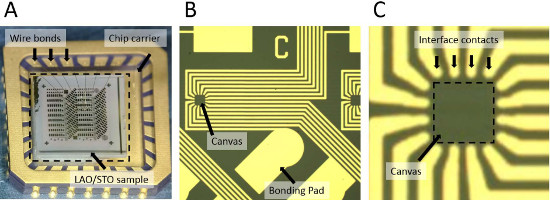
図1フォトリソグラフィ処理ステップステップ1:スピンフォトレジスト。ステップ2:マスクアライナーを用いてフォトレジストを公開します。ステップ3:フォトレジストを開発しています。ステップ4:イオンミリング。ステップ5:DCは、TiとAuを堆積させるスパッタリング。ステップ6:リフトオフ。ステップ7:第二の層を堆積させる。ステップ8:プラズマ洗浄。

図2。リソグラフィでパターンLAO / STOヘテロ構造のイメージ。チップキャリアに接合さ5mm x 5mmのサンプル線を示す(A)の画像。(B)ボンディングパッドとキャンバスの1を示す光学像。(C)単独のキャンバスのクローズアップ。 この図の拡大版を表示するには、こちらをクリックしてください。

図3。LAO / STOナノ構造の(A)非公式なデザイン。(B)は 、オープンソースのスケーラブルベクターグラフィックス(SVG)エディタを使用してナノ構造体の正確なレイアウト。

図4のC-AFMのパターニングのための(A)リソグラフィ、フロントパネル(B)3Dシミュレータからのスクリーンの位置とC-AFMチップの電圧を示す。w.jove.com/files/ftp_upload/52058/52058fig4large.jpg "ターゲット=" _blank ">この図の拡大版を表示するには、こちらをクリックしてください。

の関数としてのデバイスの四端子微分コンダクタンスの図5(A)LAO / STOナノ構造は、希釈冷凍機に挿入される。試料耐性の(B)モニタリングがmKで50 300 Kから冷却される。(C)モニタリングデバイス(V4t)全体のサイドゲート電圧VSGと電圧。強度グラフは、ジーメンス(S)の単位で表示され、電圧はボルト(V)単位で表示されている。
ディスカッション
Successful creation of nanostructures depends on several critical steps. It is important that the LAO/STO samples are grown with a thickness that is known to be at the boundary between the insulating and conductive phase. (Details of sample growth fall outside the scope of this paper, but are crucial for overall success.) Second, it is important to have relative humidity within the range 25-45% for successful c-AFM writing. Values below 25% are unlikely to produce conductive nanostructures, while too high humidity will generally produce uncontrollably large features. Also, temperature control of the AFM is important if the c-AFM tip needs to achieve precise registry over long periods of time. Once the nanostructures are created, they must be placed in a vacuum environment if experiments lasting longer than a few hours are to be performed. For the experiments described here, the structure is created and within minutes transferred to a vacuum environment.
It is recommend before writing that a “writing test” be performed on all relevant electrodes. In such a test, two virtual electrodes are first created, and a single nanowire is written while simultaneously monitoring the conductance. A similar test of erasure can be performed by “cutting” the nanowire shortly afterwards. If the nanostructure is decaying rapidly, the issue is most likely due either to the interfacial contacts or the canvas itself. To distinguish between these two effects, a four-terminal measurement of the conductance should be performed, and the two-terminal conductance should be compared with the four-terminal conductance as a function of time. If the two-terminal conductance is decaying more rapidly than the four-terminal conductance, then the issue is related to the electrical contacts to the interface. If the four-terminal conductance is decaying at a comparable rate, then most likely the canvas is not suitable and should be replaced.
There are natural limitations of the current method for creating nanostructures. Specifically, the writing speed for the smallest devices is limited to a few hundred nanometers per second. Speeds far above that value lead to unpredictable results. Use of parallel writing techniques are possible27,28, but are not highly developed and have their own drawbacks. The size of nanostructures that can be created is naturally limited by the scan range of the AFM being used. A high-quality AFM with closed-loop feedback in the two scan directions is highly recommended. Tracking of point-like objects on the sample surface should be performed to monitor temporal drift of the sample.
Once creation of conductive nanostructures at oxide interfaces has been mastered, there are a wide range of experimental directions that can be explored. Using this technique, a wide variety of nanostructures and devices have already been demonstrated, including nanowires18, tunnel barriers29, rectifying junctions30, field-effect transistors18, single-electron transistors31, superconducting nanowires32, nanoscale optical detectors33, and nanoscale THz emitters and detectors34.
開示事項
The authors have nothing to disclose.
謝辞
The long-standing collaboration with Chang-Beom Eom at the University of Wisconsin-Madison, who provided the LAO/STO samples, is gratefully acknowledged. Video editing assistance from Christopher Solis is greatly appreciated. This work is supported by NSF (DMR-1104191, DMR-1124131), ARO (W911NF-08-1-0317), and AFOSR (FA9550-10-1-0524, FA9550-12-1-0268, FA9550-12-1-0057).
資料
| Name | Company | Catalog Number | Comments |
| Equipment | |||
| Contact Aligner | Karl-Suss | MA6 | |
| Spinner | Solitec | 5110C | |
| Ion Mill | Commonwealth Scientific | 8C | |
| Sputtering System | Leybold-Heraeus | Z-650 | |
| Barrel Etcher | Branson/IPC | 3000C | |
| Wire Bonder | Westbond | 7700E | |
| AFM | Asylum Research | MFP-3D | |
| Dilution Refrigerator | Quantum Design | P850 | |
| Ultrasonic Wash Machine | Fisher Scientific | 15-335-6 | |
| Current Amplifier | Femto | DLPCA-200 | |
| Materials | |||
| LaAlO3/SrTiO3 | Prof. Chang-Beom Eom | 5 mm x 1 mm with ~3.4 unit cells of LAO (See Reference 18) | |
| Photoresist | AZ Electronic Materials | P4210 | |
| Developer | AZ Electronic Materials | 400K | |
| Acetone | Fisher Scientific | A929SK-4 | |
| Isopropyl Alcohol | Fisher Scientific | A459-1 | |
| Deionized Water | Fisher Scientific | 23-290-065 | |
| Gold Wire | DuPont | 5771 | 1 mm diameter |
| Chip Carrier | NTK Technologies | IRK28F1-5451D |
参考文献
- Sulpizio, J. A., Ilani, S., Irvin, P., Levy, J. i. . Annual Review of Materials Research, in press. , (2014).
- Mannhart, J., Blank, D. H. A., Hwang, H. Y., Millis, A. J., Triscone, J. M. Two-Dimensional Electron Gases at Oxide Interfaces. Mrs Bulletin. 33, 1027-1034 (2008).
- Zubko, P., Gariglio, S., Gabay, M., Ghosez, P., Triscone, J. -. M., Langer, J. S. Annual Review of Condensed Matter Physics. Interface Physics in Complex Oxide Heterostructures. , 141-165 (2011).
- Bogorin, D. F., Irvin, P., Cen, C., Levy, J. i., Tsymbal, E. Y., Dagotto, E. R. A., Chang-Beom, E., Ramesh, R. . Multifunctional Oxide Heterostructures. 13, (2012).
- Granozio, F. M., Koster, G., Rijnders, G. Functional Oxide Interfaces. MRS Bulletin. 38, 1017-1023 (2013).
- Ohtomo, A., Hwang, H. Y. A high-mobility electron gas at the LaAlO3/SrTiO3 heterointerface. Nature. 427, 423-426 (2004).
- Reyren, N., et al. Superconducting interfaces between insulating oxides. Science. 317, 1196-1199 (2007).
- Bark, C. W., et al. Switchable Induced Polarization in LaAlO3/SrTiO3 Heterostructures. Nano Letters. 12, 1765-1771 (2012).
- Brinkman, A., et al. Magnetic effects at the interface between non-magnetic oxides. Nature Materials. 6, 493-496 (2007).
- Thiel, S., Hammerl, G., Schmehl, A., Schneider, C. W., Mannhart, J. Tunable quasi-two-dimensional electron gases in oxide heterostructures. Science. 313, 1942-1945 (2006).
- Cen, C., et al. Nanoscale control of an interfacial metal-insulator transition at room temperature. Nature Materials. 7, 298-302 (2008).
- Singh-Bhalla, G., et al. Built-in and induced polarization across LaAlO3/SrTiO3 heterojunctions. Nature Physics. 7, 80-86 (2011).
- Li, L., et al. Very Large Capacitance Enhancement in a Two-Dimensional Electron System. Science. 332, 825-828 (2011).
- Xie, Y., Hikita, Y., Bell, C., Hwang, H. Y. Control of electronic conduction at an oxide heterointerface using surface polar adsorbates. Nature Communications. 2, 494 (2011).
- Bark, C. W., et al. Tailoring a two-dimensional electron gas at the LaAlO3/SrTiO3 (001) interface by epitaxial strain. PNAS. 108, 4720-4724 (2011).
- Tra, V. T., et al. . Adv Mater. 25, 3357-3364 (2013).
- Cronenwett, S. M., Oosterkamp, T. H., Kouwenhoven, L. P. A Tunable Kondo Effect in Quantum Dots. Science. 281, 540-544 (1998).
- Cen, C., Thiel, S., Mannhart, J., Levy, J. Oxide Nanoelectronics on Demand. Science. 323, 1026-1030 (2009).
- Kalinin, S. V., Gruverman, A. . Scanning probe microscopy: electrical and electromechanical phenomena at the nanoscale. 1, (2007).
- Piner, R. D., Zhu, J., Xu, F., Hong, S. H., Mirkin, C. A. 'Dip-pen' nanolithography. Science. 283, 661-663 (1999).
- Ahn, C. H., et al. Nonvolatile Electronic Writing of Epitaxial Pb(Zr0.52Ti0.48)O3/SrRuO3 Heterostructures. Science. 276, 1100-1103 (1997).
- Bi, F., et al. 'Water-cycle' mechanism for writing and erasing nanostructures at the LaAlO3/SrTiO3 interface. Applied Physics Letters. 97, 173110 (2010).
- Cheng, G., et al. Anomalous Transport in Sketched Nanostructures at the LaAlO3/SrTiO3 Interface. Phys Rev X. 3, 011021 (2013).
- Veazey, J. P., et al. Nonlocal current-voltage characteristics of gated superconducting sketched oxide nanostructures. Europhys Lett. 103, 57001 (2013).
- Veazey, J. P., et al. Oxide-based platform for reconfigurable superconducting nanoelectronics. Nanotechnology. 24, 375201 (2013).
- Irvin, P., et al. Anomalous High Mobility in LaAlO3/SrTiO3 Nanowires. Nano Letters. 13, 364-368 (2013).
- Salaita, K., et al. Massively Parallel Dip–Pen Nanolithography with 55 Two-Dimensional Arrays. Angewandte Chemie. 118, 7378-7381 (2006).
- Li, S., et al. Parallel Conductive-AFM Lithography on LaAlO3/SrTiO3 Interfaces. Ieee T Nanotechnol. 12, 518-520 (2013).
- Cen, C., Bogorin, D. F., Levy, J. Thermal activation and quantum field emission in a sketch-based oxide nanotransistor. Nanotechnology. 21, 475201 (2010).
- Bogorin, D. F., et al. Nanoscale rectification at the LaAlO3/SrTiO3 interface. Applied Physics Letters. 97, 013102 (2010).
- Cheng, G., et al. Sketched Oxide Single-Electron Transistor. Nature Nanotech. 6, 343-347 (2011).
- Joshua, A., Ruhman, J., Pecker, S., Altman, E., Ilani, S. Gate-tunable polarized phase of two-dimensional electrons at the LaAlO3/SrTiO3 interface. PNAS. 110, 9633 (2013).
- Irvin, P., et al. Rewritable Nanoscale Oxide Photodetector. Nature Photon. 4, 849-852 (2010).
- Ma, Y., et al. Broadband Terahertz Generation and Detection at 10 nm Scale. Nano Letters. 13, 2884-2888 (2013).
転載および許可
このJoVE論文のテキスト又は図を再利用するための許可を申請します
許可を申請さらに記事を探す
This article has been published
Video Coming Soon
Copyright © 2023 MyJoVE Corporation. All rights reserved