A subscription to JoVE is required to view this content. Sign in or start your free trial.
Method Article
Simultaneous Synthesis of Single-walled Carbon Nanotubes and Graphene in a Magnetically-enhanced Arc Plasma
In This Article
Summary
Anodic arc discharge is one of the most practical and efficient methods to synthesize various carbon nanostructures. To increase the arc controllability and flexibility, a non-uniform magnetic field was introduced to process the one-step synthesis of large-scale graphene flakes and high-purity single-walled carbon nanotubes.
Abstract
Carbon nanostructures such as single-walled carbon nanotubes (SWCNT) and graphene attract a deluge of interest of scholars nowadays due to their very promising application for molecular sensors, field effect transistor and super thin and flexible electronic devices1-4. Anodic arc discharge supported by the erosion of the anode material is one of the most practical and efficient methods, which can provide specific non-equilibrium processes and a high influx of carbon material to the developing structures at relatively higher temperature, and consequently the as-synthesized products have few structural defects and better crystallinity.
To further improve the controllability and flexibility of the synthesis of carbon nanostructures in arc discharge, magnetic fields can be applied during the synthesis process according to the strong magnetic responses of arc plasmas. It was demonstrated that the magnetically-enhanced arc discharge can increase the average length of SWCNT 5, narrow the diameter distribution of metallic catalyst particles and carbon nanotubes 6, and change the ratio of metallic and semiconducting carbon nanotubes 7, as well as lead to graphene synthesis 8.
Furthermore, it is worthwhile to remark that when we introduce a non-uniform magnetic field with the component normal to the current in arc, the Lorentz force along the J×B direction can generate the plasmas jet and make effective delivery of carbon ion particles and heat flux to samples. As a result, large-scale graphene flakes and high-purity single-walled carbon nanotubes were simultaneously generated by such new magnetically-enhanced anodic arc method. Arc imaging, scanning electron microscope (SEM), transmission electron microscope (TEM) and Raman spectroscopy were employed to analyze the characterization of carbon nanostructures. These findings indicate a wide spectrum of opportunities to manipulate with the properties of nanostructures produced in plasmas by means of controlling the arc conditions.
Protocol
1. Anode preparation
- Scale nickel powder (99.8%, 300 mesh) and yttrium powder (99.9%, 40 mesh) according to the molar radio of 4.2:1 as catalyst powder.
- Mix the catalyst powder with graphite powder (99.9995%, 200 mesh) very well. Fill the mixed powder into hollow graphite rod (5 mm outer diameter, 2.5 mm inner diameter and 75 mm length) firmly. Make sure the total molar radio of C:Ni:Y in anode rod is 94.8:4.2:1, which is optimum ratio to synthesize SWCNT 9.
- Install cathode rod (pure graphite, 13 mm diameter) and the stuffed anode rod inside cylindrical chamber (stainless steel, 152 mm diameter and 254 mm length). Adjust the gap distance between cathode and anode to about 3 mm.
2. Substrate setup
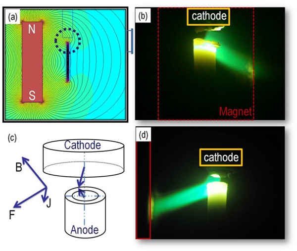
- Place a cuboid permanent magnet (25 mm × 25 mm × 100 mm) inside the chamber at about 25 mm distance from the interelectrode axis. The Ultra-High-Temp Alnico magnet used in experiment has the weight of 650 grams. Use the configuration when the interelectrode gap is placed at the distance of about h = 75 mm (Figure 1a) from the bottom of permanent magnet.
- Cut the 0.3 mm thickness molybdenum sheet (99.95%) as the 25 mm × 100 mm rectangular shape. Remove surface contamination by ultrasonic dismembrator in acetone and ethanol for 30 min with 50% sonicating amplitude, 150 w output power and 40 kHz frequency.
- Install molybdenum sheet attaching one side of permanent magnet, and turn this side towards electrodes.
- Measure the magnetic field in the interelectrode gap by a Gaussmeter. Keep the average magnetic field between the electrodes is about 0.06 T.
3. Ignition of arc plasma
- Pump down the cylindrical chamber to the pressure less than 10-1 Torr vacuum and then filled it with helium (99.995%) to 500 Torr.
- Connect arc electrodes to DC welding power supply and set up the power supply on arc current of about 75 A.
- Record the real-time values of arc current, arc voltage and chamber pressure for post-experiment analysis.
- Start the video of arcing from the right and front viewports by two digital cameras simultaneously. The snapshots after 1 second of arc starting are shown in Figure 1b (from right viewport) and Figure 1d (from front viewport).
- Run the arc for 15 seconds. Cool down chamber by natural convection for at least 20 minutes.
4. Post-synthesis analysis and characterization
- Use tweezers to tear off the deposition flake from the surface of molybdenum sheet where the arc plasmas jet was directed. Another sample is collected from the black collar of cathode. Observe the morphology of both sides of deposition flake under SEM (acceleration voltage of 30 KV was used).
- Regarding the sample preparation for TEM analysis, the thin films of sample were obtained by drop casting a suspension of methanol-dispersed SWCNT solution after sonicating for 60 minutes using ultrasonic dismembrator with 50% sonicating amplitude. Observe the morphology of the thin film under JEOL TEM with the voltage of 100 KV after the volatilization of methanol solution. For the position of interest in sample, electron diffraction pattern can be obtained with the CCD camera length of 50 cm associated with TEM.
- Raman spectroscopy was performed on a micro-Raman system based on a 200 mW Lexel 3000 Ar ion laser (tunable single line output), with holographic optics, a 0.5 m spectrometer and a liquid nitrogen cooled CCD detector; wavelength 514 nm which corresponds to the energy of 2.33 eV. Raman measurements covered the range of 100 cm-1 to 3100 cm-1, and were carried out on the surface of graphene flakes.
5. Representative Results
The video snapshots obtained simultaneously from right and front viewports of the chamber are shown in Figure 1b, d for h = 75 mm. These images illustrate significant perturbation of arc plasma column in presence of external magnetic field in comparison with axially symmetric arc column observed in the case without a magnetic field 10.
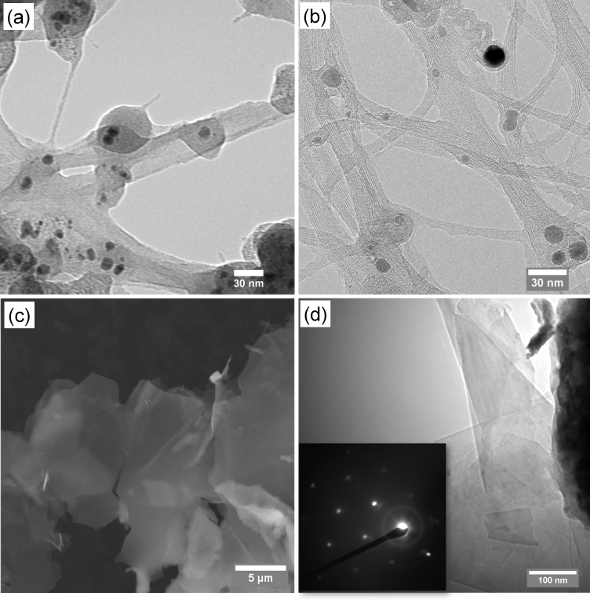
Figure 2a and 2b display the typical morphology of SWCNT and catalyst particles collected on the collar of cathode without magnetic field and with the magnetic field of B = 0.06 Tesla under TEM, respectively. It can be seen that SWCNT with magnetic field are close-packed into bundles with diameters ranging from 2 to 20 nm due to the van der Waals interaction between individual SWCNT. In comparison, the SWCNT without magnetic field have the larger diameter in bundles and larger individual diameter, which is consistent with the analysis of Raman spectrum. Also, the magnetic field can result in the SWCNT with higher purity shown in Figure 2a and 2b.
The most interesting influence of the magnetic field is that graphene flakes can be obtained from the surface of deposition flakes which is close to molybdenum sheet in the same process. Figure 2c and 2d show the SEM and TEM images of graphene flakes as well as few-layer graphene obtained from the sample taken at the location corresponded to arc plasmas jets. The inset of Figure 2d shows the electrons diffraction pattern associated with the graphene. The hexagonal dots pattern of electron diffraction presents the evidence of well-ordered crystal structures.
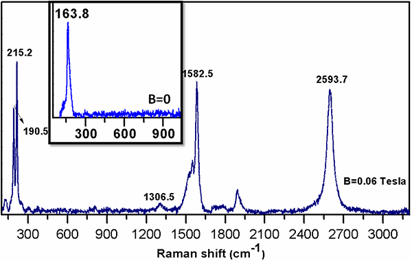
Raman spectrum is a powerful tool for characterization of graphene flakes and SWCNT. The typical peaks observed in graphene are the G and 2D peaks at ~1600 cm-1 and ~2700 cm-1 respectively, using the excitation wavelength of 514 nm. The G peak stems from in plane vibrations which can be observed in all sp2 carbon materials. The 2D peak is a second order of the D peak but is seen even in non disordered systems, due to the fourth order phonon momentum exchange double resonance process. It plays a crucial role in the characterization of graphene. The intensity I(2D)/I(G) is approximately 4 for monolayer graphene and decreases with the addition of subsequent layers, thus making it possible to estimate the thickness of graphene layers. 11 Figure 3 indicates that the value of I(2D) / I(G) is around 1, which can be the evidence of few-layer graphene. The radial breathing mode (RBM) between 120 and 350 cm-1 in Raman spectrum can be used to identify the nanotube diameter through the coherent vibration frequency of the C atoms in the radial direction. The experimental relation between the frequency and SWCNT diameter is ωRBM=A/dt+B, where the parameters of A and B equal to 234 and 10 cm-1, respectively, for the typical SWCNT formed in bundles. From Figure 3, the RBM frequencies of SWCNT without and with magnetic field are 163.8 and 215.2 cm-1, corresponding to the average individual SWCNT diameters of 1.52 and 1.14 nm, respectively.

Figure 1. Distribution of magnetic field simulated by FEMM 4.2 software (a), photograph of arc plasmas jet from the right viewport (b), schematic diagram of electrodes position and direction magnetic field in the gap for the case when the interelectrode gap is positioned about 75 mm above the bottom of permanent magnet (c), and photograph of arc plasmas jet from the front viewport (d).

Figure 2. Representative TEM image of as-synthesized SWCNT bundles without magnetic field (a) and SWCNT bundles with magnetic field (b), typical SEM image of graphene flakes synthesized with magnetic field (c), and TEM image of graphene with magnetic field. Inset is the selected area electron diffraction pattern showing the crystalline structure of graphene.

Figure 3. Raman spectrum of the samples with magnetic field in the range of 100 to 3100 cm-1. Inset: Raman spectrum of the samples without magnetic field around RBM frequencies.

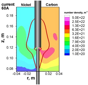
Figure 4. Nanostructure growth region and number density of carbon and nickel for arc of 60 A. Note that the densities of carbon and nickel shown on left and right hand side of the electrodes, co-exist in the same region.
Discussion
In the video snapshots shown in Figure 1b and 1d, for the case that the interelectrode gap was placed at the distance of about h=75 mm from the bottom of permanent magnet, it should be noted that change of magnet position (we tested magnet shift along z-axis and turning the magnet over) results in deviation of arc jet flow in x-direction corresponding to direction of J×B force illustrated in Figure 1c. It was also observed that the geometry of arc plasma column did...
Disclosures
We have nothing to disclose.
Acknowledgements
This work was supported by NSF/DOE Partnership in Plasma Science and Technology (NSF Grant No. CBET-0853777 and DOE Grant No. DE-SC0001169), STTR Phase I project (NSF STTR PHASE I No.1010133). The authors would like to thank the PPPL Offsite Research Program supported by the Office of Fusion Energy Sciences for supporting arc experiments.
Materials
| Name | Company | Catalog Number | Comments |
| Table of specific reagents and equipment: | |||
| Methanol | Acros Organics | 423950010 | |
| Nickel powder | Alfa Aesar | 10581 | |
| Yttrium powder | Acros Organics | 318060050 | |
| Graphite powder | Alfa Aesar | 40799 | |
| Hollow graphite rod | Saturn Industries | POCO EDM 3 | |
| Permanent magnet | McMaster-Carr | 57315K51 | |
| Molybdenum sheet | Dingqi Sci. and Tech. | 080504-11 | |
| Ultrasonic dismembrator | Fisher Scientific | Model 150T | |
| Hall-effect gaussmeter | AI | Model 100 | |
| Welding power supply | Miller | Gold Star 600SS | |
| Vacuum pump | J/B | DV-85N | |
| SEM | Carl Zeiss, Inc. | LEO 1430VP | |
| TEM | JEOL | 1200 EX | |
| Raman | Horiba Instruments Inc | HR800 | |
References
- Dai, H. J. Electrical transport properties and field effect transistors of carbon nanotubes. Nano. 1, 1-13 (2006).
- Lai, K. W. C., Xi, N., Fung, C. K. M., Chen, H. Z., Tarn, T. J. Engineering the band gap of carbon nanotube for infrared sensors. Applied Physics Letters. 95, 221107-221107 (2009).
- Gabor, N. M., Zhong, Z. H., Bosnick, K., Park, J., McEuen, P. L. Extremely Efficient Multiple Electron-Hole Pair Generation in Carbon Nanotube Photodiodes. Science. 325, 1367-1371 (2009).
- Liu, C. Hydrogen storage in single-walled carbon nanotubes at room temperature. Science. 286, 1127-1129 (1999).
- Keidar, M. Magnetic-field-enhanced synthesis of single-wall carbon nanotubes in arc discharge. Journal of Applied Physics. 103, 094318-094318 (2008).
- Li, J., Volotskova, O., Shashurin, A., Keidar, M. Controlling Diameter Distribution of Catalyst Nanoparticles in Arc Discharge. Journal of Nanoscience and Nanotechnology. 11, 10047-10052 (2011).
- Volotskova, O. Tailored Distribution of Single-Wall Carbon Nanotubes from Arc Plasma Synthesis Using Magnetic Fields. Acs. Nano. 4, 5187-5192 (2010).
- Volotskova, O. Single-step synthesis and magnetic separation of graphene and carbon nanotubes in arc discharge plasmas. Nanoscale. 2, 2281-2285 (2010).
- Farhat, S., Scott, C. D. Review of the arc process modeling for fullerene and nanotube production. Journal of Nanoscience and Nanotechnology. 6, 1189-1210 (2006).
- Keidar, M. Increasing the length of single-wall carbon nanotubes in a magnetically enhanced arc discharge. Applied Physics Letters. 92, 043129-043129 (2008).
- Ferrari, A. C. Raman spectrum of graphene and graphene layers. Physical Review Letters. 97, 187401-187401 (2006).
Reprints and Permissions
Request permission to reuse the text or figures of this JoVE article
Request PermissionExplore More Articles
This article has been published
Video Coming Soon
Copyright © 2025 MyJoVE Corporation. All rights reserved