
A subscription to JoVE is required to view this content. Sign in or start your free trial.
Method Article
Fabricating Reactive Surfaces with Brush-like and Crosslinked Films of Azlactone-Functionalized Block Co-Polymers
In This Article
Summary
Surface fabrication methods for patterned deposition of nanometer thick brushes or micron thick, crosslinked films of an azlactone block co-polymer are reported. Critical experimental steps, representative results, and limitations of each method are discussed. These methods are useful for creating functional interfaces with tailored physical features and tunable surface reactivity.
Abstract
In this paper, fabrication methods that generate novel surfaces using the azlactone-based block co-polymer, poly (glycidyl methacrylate)-block-poly (vinyl dimethyl azlactone) (PGMA-b-PVDMA), are presented. Due to the high reactivity of azlactone groups towards amine, thiol, and hydroxyl groups, PGMA-b-PVDMA surfaces can be modified with secondary molecules to create chemically or biologically functionalized interfaces for a variety of applications. Previous reports of patterned PGMA-b-PVDMA interfaces have used traditional top-down patterning techniques that generate non-uniform films and poorly controlled background chemistries. Here, we describe customized patterning techniques that enable precise deposition of highly uniform PGMA-b-PVDMA films in backgrounds that are chemically inert or that have biomolecule-repellent properties. Importantly, these methods are designed to deposit PGMA-b-PVDMA films in a manner that completely preserves azlactone functionality through each processing step. Patterned films show well-controlled thicknesses that correspond to polymer brushes (~90 nm) or to highly crosslinked structures (~1-10 μm). Brush patterns are generated using either the parylene lift-off or interface directed assembly methods described and are useful for precise modulation of overall chemical surface reactivity by adjusting either the PGMA-b-PVDMA pattern density or the length of the VDMA block. In contrast, the thick, crosslinked PGMA-b-PVDMA patterns are obtained using a customized micro-contact printing technique and offer the benefit of higher loading or capture of secondary material due to higher surface area to volume ratios. Detailed experimental steps, critical film characterizations, and trouble-shooting guides for each fabrication method are discussed.
Introduction
Developing fabrication techniques that allow for versatile and precise control of chemical and biological surface functionality is desirable for a variety of applications, from capture of environmental contaminants to development of next generation biosensors, implants, and tissue engineering devices1,2. Functional polymers are excellent materials for tuning surface properties through "grafting from" or "grafting to" techniques3. These approaches allow for control of surface reactivity based on the chemical functionality of the monomer and molecular weight of the polymer4,5,6. Azlactone-based polymers have been intensely studied in this context, as azlactone groups rapidly couple with different nucleophiles in ring-opening reactions. This includes primary amines, alcohols, thiols and hydrazine groups, thereby providing a versatile route for further surface functionalization7,8. Azlactone-based polymer films have been employed in different environmental and biological applications including analyte capture9,10, cell culture6,11, and anti-fouling/anti-adhesive coatings12. In many biological applications, patterning azlactone polymer films at nano to micrometer length scales is desirable to facilitate spatial control of biomolecule presentation, cellular interactions, or to modulate surface interactions13,14,15,16,17,18. Therefore, fabrication methods should be developed to offer high pattern uniformity and well-controlled film thickness, without compromising chemical functionality19.
Recently, Lokitz et al. developed a PGMA-b-PVDMA block copolymer which was capable of manipulating surface reactivity. PGMA blocks couple to oxide-bearing surfaces, yielding high and tunable surface densities of azlactone groups20. Previously reported methods for patterning this polymer for creation of biofunctional interfaces used traditional top-down photolithography approaches that generated non-uniform polymer films with background regions contaminated with residual photoresist material, causing high levels of non-specific chemical and biological interactions21,22,23. Here, attempts to passivate background regions caused cross-reaction with azlactone groups, compromising polymer reactivity. Considering these limitations, we recently developed techniques for patterning brush (~90 nm) or highly crosslinked (~1-10 μm) films of PGMA-b-PVDMA into chemically or biologically inert backgrounds in a manner that completely preserves the chemical functionality of the polymer24. These presented methods utilize parylene lift-off, interface-directed assembly (IDA), and custom microcontact printing (μCP) techniques. Highly detailed experimental methods for these patterning approaches, as well as critical film characterizations and challenges and limitations associated with each technique are presented here in written and video format.
Access restricted. Please log in or start a trial to view this content.
Protocol
1. PGMA-b-PVDMA Synthesis20
- Synthesis of PGMA macro-chain transfer agent (Macro-CTA)
- Use a 250-mL round-bottom reaction flask equipped with a polytetrafluoroethylene-coated magnetic stir bar.
- Combine 14.2 g of glycidyl methacrylate GMA (142.18 g/mol) with 490.8 mg of 2-cyano-2-propyl dodecyl trithiocarbonate (CPDT) (346.63 g/mol), and 87.7 mg of 2,2′-azobis (4-methoxy-2,4-dimethyl valeronitrile) (V-70) (308.43 g/mol) (molar ratio of CPDT: V-70 = 5:1), and benzene (100 mL) into air free round bottom flask.
- Degas the reaction mixture using argon and stir for 30 min. Subsequently put the solution in a temperature-controlled oil bath at 30 °C and react for 18 h.
NOTE: The targeted molecular weight for the Macro-CTA is 10,000 g/mol. 18 hours was determined to be the time necessary to reach reasonable conversion. The color of the polymer solution is transparent light yellow. - After 18 h, terminate the reaction by submerging the round bottom flask in liquid N2.
- Precipitate the polymer by pouring the light-yellow solution of polymer/benzene (~100 mL) into 400 mL of hexane.
- Stir the mixture for 5 min. Precipitate will be settled at the bottom of the beaker and is recovered by filtration.
- Dry the precipitate overnight under vacuum. Then dilute it in 400 mL of tetrahydrofuran (THF). Re-precipitate in hexane.
- Dry this new precipitate again with argon overnight.
NOTE: Macro-CTA is a fine yellow powder. The product yield of the reaction will be ~43.8%. The Mn of the PGMA Macro-CTA is 7,990 g/mol with a polydispersity (PDI) of 1.506 (MW = 12,030 g/mol).
- Synthesis of PGMA-b-PVDMA
- Fractionally distill the VDMA under reduced pressure, and reserve the middle fraction (~70%) for use.
NOTE: This is required to remove polymerization inhibitor. The distillation apparatus is attached to a Schlenk line and the air seal valve is partially opened to the vacuum line. Minimal heat is applied using a varistat and heating mantle until the VDMA monomer begins distilling over at a rate of 1 drop per second. - Combine the 2-Vinyl-4,4- dimethyl azlactone (VDMA) (139.15 g/mol)monomer (10.436 g) with the PGMA-macroCTA (1.669 g), V-70 (14.5 mg; molar ratio of PGMA-macroCTA: V-70 = 3:1) and benzene (75.0 mL) in a single-neck 250-mL round-bottom reaction flask equipped with a Teflon-coated magnetic stir bar.
NOTE: Molecular weight information, PVDMA: 139.15 g/mol, PGMA-macroCTA: 12,030 g/mol, Benzene: 78.11 g/mol. - Degas the mixture with high purity argon and stir for 30 min, and then put in oil bath at 32 °C for 18 h.
- Terminate the reaction by submerging the round bottom flask in liquid N2.
- Precipitate the polymer three times into hexane and dry it at room temperature under vacuum.
- Characterize the molecular weight and PDI of the product by using size exclusion chromatography (S) (see the Table of Materials) according to the procedure in Lokitz et al.20.The size exclusion chromatograph (S) is equipped with three PLgel 5 µm mixed-C columns (300 x 7.5 mm) in series, a refractive index detector (Wavelength= 880 nm), a photodiode array detector, multi-angle light scattering (MALS) detector (Wavelength= 660 nm), and a viscometer (see the Table of Materials).
NOTE: All experiments performed in this manuscript used product with PGMA and PVDMA block lengths of 56 and 175, respectively. The molecular weight of the block copolymer was 37,620 g/mol and the PDI was 1.16.
- Fractionally distill the VDMA under reduced pressure, and reserve the middle fraction (~70%) for use.
2. Generation of Parylene Stencil Patterns Over Silicon Substrates
- Parylene coating
- Sonicate silicon wafers in 50% wt. acetone in water for 5 min followed by sonication in 50% wt. isopropanol (IPA) in water for 5 min.
- Rinse silicon wafers with deionized (DI) water and blow dry with nitrogen gas.
- Deposit 80 nm and 1 µm thick parylene N on 4-inch silicon wafers using a parylene coater (see the Table of Materials).
NOTE: Characterize the thickness of parylene films by using a surface profilometer (see the Table of Materials).- Calibrate parylene film thickness with parylene dimer mass for each individual parylene coating system.
NOTE: In the current system, ~80 mg and ~1000 mg parylene N dimer was required to obtain 80 nm and 1 µm film thickness, respectively (based on the calibration curve obtained). - Use the following settings during operation of the parylene coater: pressure: 80 mTorr, duration: 1 h, furnace temperature: 690 °C, vaporizer temperature: 160 °C.
- Calibrate parylene film thickness with parylene dimer mass for each individual parylene coating system.
- Photolithography
- Bake wafers in an oven at 100 °C for 20 min; then let wafers sit for another 3 min at room temperature.
NOTE: Additional wait time improves adhesion of the photoresist. - Add 2 mL of positive photoresist (see the Table of Materials) and dispense at the center of the parylene-coated wafer. Spin coat the wafers at 3000 rpm for 30 s.
NOTE: Spin coating must be done under the hood. - Wait 1 min, bake wafer on a hot plate at 105 °C for 1 min.
- Load photomask in a mask alignment system (see the Table of Materials). Expose wafers to UV light (λ=325 nm) for 10 s with a dosage of 65 mJ/cm2.
- Let the wafers sit for another 5 min at room temperature.
- Develop wafers by submerging in developer (see the Table of Materials) solution for 2 min. Rinse the wafers with deionized water, and then dry with N2. Do this under the hood.
NOTE: After developing, photoresist appears completely removed from areas exposed to UV. Use an optical microscope (see the Table of Materials) to verify the wafers.
- Bake wafers in an oven at 100 °C for 20 min; then let wafers sit for another 3 min at room temperature.
- Reactive ion etching
- Use a reactive ion etching (RIE) tool (see the Table of Materials) to etch developed wafers with oxygen plasma.
- Apply an oxygen flow rate of 50 cm3/min at a chamber pressure of 20 mTorr.
- For a parylene film thickness of 1 µm, use RF power of 50 W and inductively coupled plasma (ICP) power of 500 W for 100 s was to remove exposed parylene from patterned areas. This corresponded to a parylene etch rate of 1.0-1.15 µm/min.
- For a parylene thickness of 80 nm, use RF power of 50 W and ICP power of 200 W for 55 s to remove exposed parylene from patterned areas. This corresponds to a parylene etch rate of 570-620 nm/min.
NOTE: For efficient parylene removal, determine the parylene etch rate for each RIE system. - Inspect etched substrates with an optical microscope. The silicon surface will appear shiny after the parylene is completely removed from exposed regions.
- Verify etch depth using a surface profilometer (see the Table of Materials).
3. Parylene Lift-off Procedure
- Preparation of polymer solutions
- Dissolve PGMA-b-PVDMA into chloroform (1% wt.). Chloroform should be anhydrous to prevent hydrolysis of azlactone groups.
NOTE: Chloroform is the preferred solvent because it has a high degree of solubility for the polymer, allowing for more uniform surface deposition of single polymer chains compared to other organic solvents25.
- Dissolve PGMA-b-PVDMA into chloroform (1% wt.). Chloroform should be anhydrous to prevent hydrolysis of azlactone groups.
- Cleaning parylene stencils with the plasma cleaner
- Turn on the plasma cleaner (see the Table of Materials) main power and put the parylene-coated substrates in the plasma cleaner chamber.
- Turn on the vacuum pump and evacuate the air in the chamber until the pressure gauge is less than 400 mTorr.
- Slightly open the metering valve and allow the air to enter to the plasma cleaner until the pressure gauge shows 800-1000 mTorr.
- Select RF with Hi mode and expose the substrates for 3 min.
- At the end of process, turn off the RF power and vacuum pump.
- Turn off the plasma cleaner and remove the substrates.
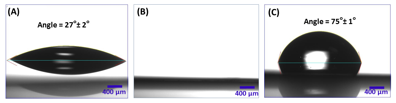
NOTE: After plasma cleaning, the surface shows hydrophilic behavior (Figure 1B) . The water contact angle of bare silicon surfaces before and after plasma cleaning are 27° ± 2° and 0°, respectively.
- Spin-coating of PGMA-b-PVDMA, annealing and sonication over the parylene stencils
- Immediately spin-coat the substrates with 100 µL of 1% wt. PGMA-b-PVDMA in anhydrous chloroform at 1500 rpm, for 15 s using a spin coater (see the Table of Materials).
NOTE: Perform spin-coating within 1-2 s of pipetting the polymer solution to minimize film non-uniformity caused by rapid chloroform evaporation. - Anneal the polymer films at 110 °C in a vacuum oven (see the Table of Materials) for 18 h.
NOTE: Annealing allows for polymer microphase segregation and surface attachment of the GMA block to the surface26.- After the annealing, characterize the polymer coating by measuring the contact angle of substrates. Surfaces show a contact angle of 75°± 1° (Figure 1C)20.
- Sonicate the substrates in 20 mL of acetone or chloroform for 10 min to remove the parylene layer and any physisorbed polymer.
NOTE: Use the following sonication conditions: ultra sonic power, 284 W; Operating frequency, 40 kHz (see the Table of Materials).
NOTE: Parylene can also be peeled off the substrate by applying a piece of Scotch tape at the edge of the substrate then pulling the tape away27. - Store the substrates under vacuum in a desiccator until characterization.
- Immediately spin-coat the substrates with 100 µL of 1% wt. PGMA-b-PVDMA in anhydrous chloroform at 1500 rpm, for 15 s using a spin coater (see the Table of Materials).

Figure 1: Contact angle measurements for treated silicon substrates. (A) Bare silicon, (B) Plasma-cleaned silicon, (C) Spin-coated silicon with PGMA-b-PVDMA (after annealing and sonication in chloroform). Please click here to view a larger version of this figure.
4. PGMA-b-PVDMA Interface-Directed Assembly Procedure
NOTE: This procedure can be performed on substrates containing either a chemically inert background (section 4.1), or a biologically inert background (section 4.2), depending on the application.
- Preparation of chemically inert background on silicon substrates
- Use oxygen plasma cleaner to clean the bare silicon (section 3.2).
- Pipette 100 µL of trichloro(1H,1H,2H,2H-perfluorooctyl) silane (TPS) onto a Petri dish and place the silicon substrates inside a vacuum desiccator next to the Petri dish.
- Apply vacuum (-750 Torr) for 1 h for chemical vapor deposition (CVD).
CAUTION: TPS is highly toxic and the CVD process should be performed inside a fume hood.
NOTE: After 1 h the substrate shows hydrophobic behavior. A contact angle of 109°± 3° is typically measured after the CVD process. The thickness of the TPS film is 1.5 ± 0.5 nm.
NOTE: TPS blocks reaction of the reactive surface oxide with PGMA-b-PVDMA. - Coat the wafers with parylene (1 µm thickness). Perform photolithography and reactive ion etching to generate parylene patterns (section 2) and to etch away the TPS layer in the exposed regions.
- Preparation of polyethylene glycol (PEG) background on silicon substrates.
- Use the oxygen plasma cleaner for 3 min to clean the bare silicon substrates (section 3.2).
- Perform CVD of TPS for 1 h (section 4.1.2).
- Immerse substrates into a 0.7% wt/v solution of Pluronic F-127 in ultrapure water for 18 h to generate a PEG layer on the surface28,29.
NOTE: Pluronic contains a hydrophobic polypropylene oxide (PPO) polymer block between two PEG chains. The PPO block anchors the polymer to the TPS surface while the PEG chains are exposed to solution28. - Wash and rinse the substrate for 5 min with 100 mL of ultrapure water.
- Deposit 80 nm and 1 µm thick parylene N on 4-inch silicon wafers using a parylene coater.
- Perform photolithography and reactive ion etching to generate parylene patterns (section 2).
- Sonication, spin-coating of PGMA-b-PVDMA polymer, and annealing the substrates
- Sonicate chemically inert (TPS) substrates (section 4.1) or PEG-functional substrates (section 4.2) for 10 min in acetone to remove the parylene layer.
- Spin-coat the sonicated substrate with 100 µL of 1% wt. PGMA-b-PVDMA in anhydrous chloroform at 1500 rpm for 15 s.
- Anneal the polymer films at 110 °C under vacuum for 18 h.
- Sonicate the substrates in acetone or chloroform for 10 min to remove physisorbed polymer present in background regions on the surface.
- Store the substrates in a vacuum desiccator until further use.
5. Custom PGMA-b-PVDMA Micro-Contact Printing (μCP)
- PDMS stamp fabrication
- Fabricate the silicon masters according to the standard photolithography procedure30. Use CVD process (section 4.1.2) to deposit anti-adhesive TPS onto the silicon masters.
NOTE: The silicon mold should be treated with TPS the first time it is used, and re-applied after it has been used 5-10 times. - Perform standard soft lithography methods for fabrication of stamps (PDMS precursor to curing agent mass ratio 10:1)31.
NOTE: Stamps used in this study consist of micropillar arrays (diameter = 5-50 µm, height = 20 µm). - Cut out a single stamp. Clean the stamp by sonicating for 10 min in HCl (1 M), 5 min in acetone, followed by 5 min in ethanol.
- Dry the stamps in a convection oven at 80 °C for 20 min to remove residual organic solvent.
- Fabricate the silicon masters according to the standard photolithography procedure30. Use CVD process (section 4.1.2) to deposit anti-adhesive TPS onto the silicon masters.
- Microcontact printing of PGMA-b-PVDMA onto silicon substrates
- Deposit TPS onto the surface of PDMS stamps using the CVD process (section 4.1.2).
NOTE: The TPS layer is used to prevent coupling of the polymer to the stamp surface.
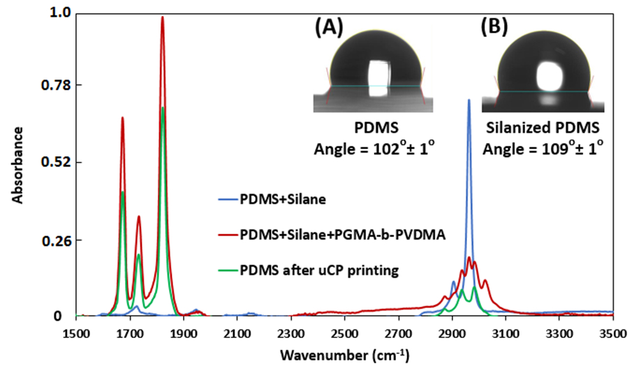
NOTE: Contact angle measurements can be used to characterize stamps after TPS adsorption, as shown in Figure 2 (Inset A, B). - Dissolve the PGMA-b-PVDMA polymer into anhydrous chloroform at a concentration of 0.25-1% wt.
- Submerge the stamps into 5 mL of the polymer solution for 3 min.
- Plasma clean 2×2 cm bare silicon substrates for 3 min to clean surface for coupling with the PGMA blocks (section 3.2).
- Take out the polymer-coated stamps from the polymer solution.
NOTE: Stamps must be used for printing while they are still wet and a layer of solution exists over them. - Put inked stamp directly on silicon substrate.
- Use a manual drill press stand (see the Table of Materials) (Figure 3) to press the polymer-coated stamps onto the silicon surface to promote pattern transfer. Immediately apply the stamp to the substrate (within 1-2 s) after taking out the coated stamps from polymer solution.
NOTE: Both the silicon and the PDMS stamp can be placed on double-sided tape backing to minimize PDMS stamp deformation due to non-uniform or high pressure stamping32. - Apply conformal contact between polymer-inked stamp and silicon substrate for 1 min. Use the estimated pressure of 75 g/cm2(7.35 kPa) to press.
- Gently separate the stamp from the silicon surface.
- Anneal the printed silicon substrates immediately in a vacuum oven at 110 °C for 18 h.
- Sonicate the printed silicon substrates in acetone or chloroform for 10 min to remove any physically-adsorbed PGMA-b-PVDMA and then dry with N2.
- Perform surface characterization analysis for both PDMS stamp (after printing step) and printed-silicon (after annealing and sonication steps) to verify the successful transfer of PGMA-b-PVDMA.
NOTE: Surface profilometer and attenuated total reflectance Fourier-transform infrared spectroscopy (ATR-FTIR) analysis could be used to analyze the printed-silicon substrate and PDMS stamp, respectively.
- Perform surface characterization analysis for both PDMS stamp (after printing step) and printed-silicon (after annealing and sonication steps) to verify the successful transfer of PGMA-b-PVDMA.
- Store the substrates under vacuum in a desiccator until characterization.
- Deposit TPS onto the surface of PDMS stamps using the CVD process (section 4.1.2).

Figure 2: ATR-FTIR measurements for treated PDMS stamps (Relative intensity). (Inset A) Contact angle measurements for bare PDMS stamp. (Inset B) Contact angle measurements for TPS treated PDMS stamp. Please click here to view a larger version of this figure.

Figure 3: Setup for μCP of PGMA-b-PVDMA solutions onto silicon substrates. The procedure includes use of a (A) manual drill press, (B) a TPS-functionalized PDMS stamp coated with the PGMA-b-PVDMA polymer, (C) a plasma cleaned 2×2 cm silicon substrate, and (D) double-sided tape.
Access restricted. Please log in or start a trial to view this content.
Results
Contact angle measurements can be used to evaluate the functionalization of silicon with PGMA-b-PVDMA. Figure 1 depicts the contact angle of the silicon substrate during the different processing steps. Hydrophilic behavior of the plasma cleaned silicon substrate is shown in Figure 1B. The contact angle after polymer spin coating and annealing is 75° ± 1°(Figure 1C)...
Access restricted. Please log in or start a trial to view this content.
Discussion
This article presents three approaches to patterning PGMA-b-PVDMA, each with its set of advantages and drawbacks. The parylene lift-off method is a versatile method for patterning block co-polymers at micro to nanoscale resolution, and has been used as a deposition mask in other patterning systems33,34,35. Due to its relatively weak surface adhesion, the parylene stencil can be easily removed from the surface by sonicat...
Access restricted. Please log in or start a trial to view this content.
Disclosures
The authors have nothing to disclose.
Acknowledgements
This research was supported by Kansas State University. A portion of this research was conducted at the Center for Nanophase Materials Sciences, which is sponsored at Oak Ridge National Laboratory by the Scientific User Facilities Division, Office of Basic Energy Sciences and U.S. Department of Energy.
Access restricted. Please log in or start a trial to view this content.
Materials
| Name | Company | Catalog Number | Comments |
| Material | |||
| Ethanol, ≥ 99.5% | Sigma-Aldrich | 459844 | - |
| HCL, 1.019 N in H2O | Fluka Analytical | 318949 | - |
| Acetone, ≥ 99.5% | Sigma-Aldrich | 320110 | - |
| Benzene, ≥ 99.9% | Sigma-Aldrich | 270709 | - |
| Isopropanol, ACS reagent, ≥99.5% | Sigma-Aldrich | 190764 | |
| Hexane | Fisher Chemical | H292-4 | - |
| Argon | Matheson Gas | G1901175 | - |
| Tetrahydrofuran (THF), ≥ 99.9% | Sigma-Aldrich | 401757 | - |
| Pluronic F-127 | Sigma-Aldrich | P2443 | - |
| Polydimethyl Siloxane (PDMS) Slygard 184 | Dow Corning | 4019862 | - |
| Trichloro (1H,1H,2H,2H-perfluorooctyl) silane (TPS), 97% | Sigma-Aldrich | 448931 | It is toxic. Work with it under hood |
| Anhydrous Chloroform, ≥ 99% | Sigma-Aldrich | 372978 | - |
| Positive Photoresist AZ1512 | MicroChemicals | AZ 1512 | amber-red liquid, density 1.083 g/cm3, spin coating step should be done under the hood |
| Developer AZ 300 MIF | MicroChemicals | AZ300 MIF | clear colourless liquid with slight amine odor and density of 1 g/cm3 |
| 1,2-Vinyl-4,4- dimethyl azlactone (VDMA) | Isochem North America, LLC | VDMA | - |
| 2-cyano-2-propyl dodecyl trithiocarbonate (CPDT) | Sigma-Aldrich | 723037 | - |
| 2,2′-Azobis (4methoxy-2,4-dimethyl valeronitrile) (V-70) | Wako Specialty Chemicals | CAS NO. 15545-97-8, EINECS No. 239-593-8 | - |
| Parylene N | Specialty Coating Systems | 15B10004 | - |
| Name | Company | Catalog Number | Comments |
| Equipment | |||
| Parylene Coater | Specialty Coating Systems | SCS Labcoater (PDS 2010) | - |
| Mask alignment system | Neutronix Quintel | NXQ8000 | - |
| Oxygen Plasma Etcher | Oxford Instruments | Plasma Lab System 100 | - |
| Surface Profilometer | Veeco | Dektak 150 | Scan type was standard hill. Scan duration and force were 120 s and 1 mg, respectively. |
| Brightfield Upright Microscope | Olympus Corporation | BX51 | - |
| Oxygen Plasma Cleaner | Harrick Plasma | PDC-001-HP | - |
| Attenuated Total Reflectance Fourier Transform Infrared Spectroscopy (ATR-FTIR) | Perkin Elmer | ATR-FTIR 100 | - |
| Atomic Force Microscopy (AFM) | PicoPlus | Picoplus atomic force microscope | Veeco MLCT-E cantilevers with a 0.5 N/m spring constant. Scan speeds varied between 0.25 and 1 Hz. |
| Scanning Electron Microscopy (SEM) | Hitachi Science Systems Ltd., Tokyo, Japan | - | - |
| Rotary Tool Workstation | Dremel | Model 220-01 | - |
| Spin Coater | Smart Coater | SC100 | - |
| Vacuum Oven | Yamato Scientific Co. | PCD-C6(5)000) | - |
| Size Exclusion Chromatography (SEC) | Waters Alliance 2695 Separations Module | 720004547EN | - |
| Refractive Index (RI) detector | Waters | Model 2414 | - |
| Photodiode Array Detector | Waters | Model 2996, 716001286 | - |
| Multi-angle Light Scattering (MALS) Detector | Wyatt Technology | miniDAWN TREOS II | - |
| Viscometer | Wyatt Technology | Viscostar | - |
| PLgel 5 µm mixed-C columns (300 x 7.5 mm) | Agilent | 5 µm mixed-C columns | - |
| Ellipsometer | J. A. Woollam | alpha-SE | Cauchy model, PGMA and PVDMA layers had refractive indices of 1.50 and 1.52 at 632 nm |
| Ultrasonic Sonicator | Fischer Scientific | FS-110H | - |
References
- Faia-Torres, A., Goren, T., Textor, M., Pla-Roca, M. Patterned Biointerfaces. Comprehensive biomaterials. , 1st edition, Elsevier publications. 181-201 (2017).
- Ogaki, R., Alexander, M., Kingshott, P. Chemical patterning in biointerface science. Materials Today. 13 (4), 22-35 (2010).
- Rungta, A., et al. Grafting bimodal polymer brushes on nanoparticles using controlled radical polymerization. Macromolecules. 45 (23), 9303-9311 (2012).
- Guyomard, A., Fournier, D., Pascual, S., Fontaine, L., Bardeau, J. Preparation and characterization of azlactone functionalized polymer supports and their application as scavengers. European Polymer Journal. 40 (10), 2343-2348 (2004).
- Zayas-Gonzalez, Y. M., Lynn, D. M. Degradable Amine-Reactive Coatings Fabricated by the Covalent Layer-by-Layer Assembly of Poly (2-vinyl-4, 4-dimethylazlactone) with Degradable Polyamine Building Blocks. Biomacromolecules. 17 (9), 3067-3075 (2016).
- Schmitt, S. K., et al. Peptide Conjugation to a Polymer Coating via Native Chemical Ligation of Azlactones for Cell Culture. Biomacromolecules. 17 (3), 1040-1047 (2016).
- Yu, Q., Cho, J., Shivapooja, P., Ista, L. K., López, G. P. Nanopatterned smart polymer surfaces for controlled attachment, killing, and release of bacteria. ACS Applied Materials & Interfaces. 5 (19), 9295-9304 (2013).
- Jones, M. W., Richards, S., Haddleton, D. M., Gibson, M. I. Poly (azlactone)s: versatile scaffolds for tandem post-polymerisation modification and glycopolymer synthesis. Pilymer Chemistry UK. 4 (3), 717-723 (2013).
- Barkakaty, B., et al. Amidine-Functionalized Poly (2-vinyl-4, 4-dimethylazlactone) for Selective and Efficient CO2 Fixing. Macromolecules. 49 (5), (2016).
- Cullen, S. P., Mandel, I. C., Gopalan, P. Surface-anchored poly (2-vinyl-4, 4-dimethyl azlactone) brushes as templates for enzyme immobilization. Langmuir. 24 (23), 13701-13709 (2008).
- Schmitt, S. K., et al. Polyethylene glycol coatings on plastic substrates for chemically defined stem cell culture. Advanced Healthcare Materials. 4 (10), 1555-1564 (2015).
- Yan, S., et al. Nonleaching Bacteria-Responsive Antibacterial Surface Based on a Unique Hierarchical Architecture. ACS Applied Materials & Interfaces. 8 (37), 24471-24481 (2016).
- Li, C., et al. Creating "living" polymer surfaces to pattern biomolecules and cells on common plastics. Biomacromolecules. 14 (5), 1278-1286 (2013).
- Brétagnol, F., et al. Surface functionalization and patterning techniques to design interfaces for biomedical and biosensor applications. Plasma Processes and Polymers. (6-7), 443-455 (2006).
- Thery, M. Micropatterning as a tool to decipher cell morphogenesis and functions. Journal of Cell Science. 123 (Pt 24), 4201-4213 (2010).
- Robertus, J., Browne, W. R., Feringa, B. L. Dynamic control over cell adhesive properties using molecular-based surface engineering strategies. Chemical Soceity Reviews. 39 (1), 354-378 (2010).
- Kane, R. S., Takayama, S., Ostuni, E., Ingber, D. E., Whitesides, G. M. Patterning proteins and cells using soft lithography. Biomaterials. 20 (23), 2363-2376 (1999).
- Cattani-Scholz, A., et al. PNA-PEG modified silicon platforms as functional bio-interfaces for applications in DNA microarrays and biosensors. Biomacromolecules. 10 (3), 489-496 (2009).
- Nie, Z., Kumacheva, E. Patterning surfaces with functional polymers. Nature Materials. 7 (4), (2008).
- Lokitz, B. S., et al. Manipulating interfaces through surface confinement of poly (glycidyl methacrylate)-block-poly (vinyldimethylazlactone), a dually reactive block copolymer. Macromolecules. 45 (16), 6438-6449 (2012).
- Kratochvil, M. J., Carter, M. C., Lynn, D. M. Amine-Reactive Azlactone-Containing Nanofibers for the Immobilization and Patterning of New Functionality on Nanofiber-Based Scaffolds. ACS Applied Materials & Interfaces. 9 (11), 10243-10253 (2017).
- Wancura, M. M., et al. Fabrication, chemical modification, and topographical patterning of reactive gels assembled from azlactone-functionalized polymers and a diamine. Journal of Polymer Science Part A1. 55 (19), 3185-3194 (2017).
- Hansen, R. R., et al. Lectin-functionalized poly (glycidyl methacrylate)-block-poly (vinyldimethyl azlactone) surface scaffolds for high avidity microbial capture. Biomacromolecules. 14 (10), 3742-3748 (2013).
- Masigol, M., Barua, N., Retterer, S. T., Lokitz, B. S., Hansen, R. R. Chemical copatterning strategies using azlactone-based block copolymers. Journal of Vacuum Science and TechnologyB. 35 (6), 06GJ01(2017).
- Lokitz, B. S., et al. Dilute solution properties and surface attachment of RAFT polymerized 2-vinyl-4, 4-dimethyl azlactone (VDMA). Macromolecules. 42 (22), 9018-9026 (2009).
- Aden, B., et al. Assessing Chemical Transformation of Reactive, Interfacial Thin Films Made of End-Tethered Poly (2-vinyl-4, 4-dimethyl azlactone)(PVDMA) Chains. Macromolecules. 50 (2), 618-630 (2017).
- Hansen, R. H., et al. Stochastic assembly of bacteria in microwell arrays reveals the importance of confinement in community development. Public Library of Science One. 11 (5), e0155080(2016).
- Vargis, E., Peterson, C. B., Morrell-Falvey, J. L., Retterer, S. T., Collier, C. P. The effect of retinal pigment epithelial cell patch size on growth factor expression. Biomaterials. 35 (13), 3999-4004 (2014).
- Tzvetkova-Chevolleau, T., et al. Microscale adhesion patterns for the precise localization of amoeba. Microelectronic Engineering. 86 (4), 1485-1487 (2009).
- Shelly, M., Lee, S., Suarato, G., Meng, Y., Pautot, S. Photolithography-Based Substrate Microfabrication for Patterning Semaphorin 3A to Study Neuronal Development. Semaphorin Signaling: Methods and Protocols. 1493, 321-343 (2017).
- McDonald, J. C., et al. Fabrication of microfluidic systems in poly(dimethylsiloxane). Electrophoresis. 21 (1), 27-40 (2000).
- Hansen, R. R., et al. High content evaluation of shear dependent platelet function in a microfluidic flow assay. Annals of Biomedical Engineering. 41 (2), 250-262 (2013).
- Segalman, R. A., Yokoyama, H., Kramer, E. J. Graphoepitaxy of spherical domain block copolymer films. Advanced Materials. 13 (15), 1152-1155 (2001).
- Stoykovich, M. P., et al. Directed assembly of block copolymer blends into nonregular device-oriented structures. Science. 308 (5727), New York, N.Y. 1442-1446 (2005).
- Craig, G. S., Nealey, P. F. Self-assembly of block copolymers on lithographically defined nanopatterned substrates. Journal of Polymer Science and Technology. 20 (4), 511-517 (2007).
- Kodadek, T. Protein microarrays: prospects and problems. Chemical Biology. 8 (2), 105-115 (2001).
- Atsuta, K., Suzuki, H., Takeuchi, S. A parylene lift-off process with microfluidic channels for selective protein patterning. Journal of Micromechanics and Microengineering. 17 (3), 496(2007).
- Ramanathan, M., Lokitz, B. S., Messman, J. M., Stafford, C. M., Kilbey, S. M. II Spontaneous wrinkling in azlactone-based functional polymer thin films in 2D and 3D geometries for guided nanopatterning. Journal of Material Chemistry C. 1 (11), 2097-2101 (2013).
- Suh, K. Y., Jon, S. Control over wettability of polyethylene glycol surfaces using capillary lithography. Langmuir. 21 (15), 6836-6841 (2005).
- Buck, M. E., Lynn, D. M. Layer-by-Layer Fabrication of Covalently Crosslinked and Reactive Polymer Multilayers Using Azlactone-Functionalized Copolymers: A Platform for the Design of Functional Biointerfaces. Advanced Engineering Materials. 13 (10), 343-352 (2011).
- Ma, L., et al. Trap Effect of Three-Dimensional Fibers Network for High Efficient Cancer-Cell Capture. Advanced Healthcare Materials. 4 (6), 838-843 (2015).
- Massad-Ivanir, N., Shtenberg, G., Tzur, A., Krepker, M. A., Segal, E. Engineering nanostructured porous SiO2 surfaces for bacteria detection via "direct cell capture". Analytical Chemistry. 83 (9), 3282-3289 (2011).
- Ilic, B., Craighead, H. Topographical patterning of chemically sensitive biological materials using a polymer-based dry lift off. Biomedical Microdevices. 2 (4), 317-322 (2000).
- Gates, B. D., et al. New approaches to nanofabrication: molding, printing, and other techniques. Chemical Reviews. 105 (4), 1171-1196 (2005).
- Jonas, U., del Campo, A., Kruger, C., Glasser, G., Boos, D. Colloidal assemblies on patterned silane layers. Proceedings of the National Academy of Sciences USA. 99 (8), 5034-5039 (2002).
- Qin, D., Xia, Y., Whitesides, G. M. Soft lithography for micro-and nanoscale patterning. Nature Protocols. 5 (3), 491-502 (2010).
Access restricted. Please log in or start a trial to view this content.
Reprints and Permissions
Request permission to reuse the text or figures of this JoVE article
Request PermissionExplore More Articles
This article has been published
Video Coming Soon
Copyright © 2025 MyJoVE Corporation. All rights reserved