
Method Article
写作和氧化物纳米结构的低温特性
摘要
Oxide nanostructures provide new opportunities for science and technology. The interfacial conductivity between LaAlO3 and SrTiO3 can be controlled with near-atomic precision using a conductive atomic force microscopy technique. The protocol for creating and measuring conductive nanostructures at LaAlO3/SrTiO3 interfaces is demonstrated.
摘要
Oxide nanoelectronics is a rapidly growing field which seeks to develop novel materials with multifunctional behavior at nanoscale dimensions. Oxide interfaces exhibit a wide range of properties that can be controlled include conduction, piezoelectric behavior, ferromagnetism, superconductivity and nonlinear optical properties. Recently, methods for controlling these properties at extreme nanoscale dimensions have been discovered and developed. Here are described explicit step-by-step procedures for creating LaAlO3/SrTiO3 nanostructures using a reversible conductive atomic force microscopy technique. The processing steps for creating electrical contacts to the LaAlO3/SrTiO3 interface are first described. Conductive nanostructures are created by applying voltages to a conductive atomic force microscope tip and locally switching the LaAlO3/SrTiO3 interface to a conductive state. A versatile nanolithography toolkit has been developed expressly for the purpose of controlling the atomic force microscope (AFM) tip path and voltage. Then, these nanostructures are placed in a cryostat and transport measurements are performed. The procedures described here should be useful to others wishing to conduct research in oxide nanoelectronics.
引言
氧化物异质1-5表现出了显着各种各样的突发物理现象这都是有趣的科学和应用4可能有用。特别是, 铝酸镧(LAO)和钛酸锶(STO)6之间的界面上可以显示出绝缘性,导电,超导7,铁电状8和9铁磁行为。在2006年,Thiel 等人发现10,有一个锐利的绝缘体-金属转变为LAO层的厚度增加时,为4的单元电池(4UC)的临界厚度。据事后证明3uc-LAO/STO结构表现出了可以在本地用导电原子力显微镜(C-AFM)探针11被控制的迟滞过渡。
氧化接口,如铝酸镧/ 钛酸锶的属性取决于传导的存在或不存在电子界面处。这些电子可以通过顶部栅电极12,13,背门10被控制,表面吸附物14,铁电层15,16和c-AFM光刻11。的C-AFM平版印刷的独特的特点是非常小的纳米级功能可以被创建。
电顶部门控,并结合2维限制,通常被用来创建在III-V族半导体17的量子点。备选地,准一维半导体纳米线可以电由接近门控。该方法用于制备这些结构是耗时的且通常不可逆的。与此相反,在C-原子力显微镜光刻技术是可逆的,即纳米结构可以为一个实验被创建,然后在"擦除"(类似白板)。通常,C-AFM写作与施加在针尖正电压进行的,而,擦除使用负电压被执行。创建特定结构所需的时间依赖于该设备的复杂性,但通常不超过30分钟;大部分时间都花在擦除画布。典型的空间分辨率约为10纳米,但2纳米可以创建18用适当的调整功能小。
纳米级的制造步骤的详细说明如下。这里所提供的细节,应足以允许类似的实验,以通过感兴趣的研究人员进行。这里所描述的方法具有超过用于在半导体制造的电子的纳米结构的传统光刻方法的许多优点。
这里所描述的C-AFM光刻方法是一个更广泛的类的扫描探针为基础的光刻技术的努力,包括扫描阳极氧化19,蘸笔纳米光刻20,压电图案的一部分21,依此类推。这里所描述的C-原子力显微镜技术,再加上使用的新型氧化物界面,可以产生一些最精密的电子结构与前所未有的各种物理性能。
研究方案
1,获取LAO / STO异质
- 获得氧化物异质结构由老挝3.4单位细胞对TiO 2结尾的STO基片脉冲激光沉积生长的。样品成长之详情载于文献22中描述。
2,光刻样品的处理
建立电接触到老挝/ STO界面,与焊盘布线画布到芯片载体。各个处理步骤的详细说明如下。
- 旋光刻胶
- 旋转光致抗蚀剂上的样品,在600 rpm离心5秒,然后在4,000 rpm下进行30秒。光致抗蚀剂层将约2微米厚。烤的试样在95℃下1分钟。
- 使用掩模对准器320处的光线为100秒为5毫瓦/厘米2的剂量曝光光致抗蚀剂。
- 开发在光致抗蚀剂显影剂的光致抗蚀剂FO中R 1分钟。
- 离子铣削
- 使用氩离子磨到不属于光致抗蚀剂的区域去除材料的15纳米(LAO和STO)。将样品在一个22.5°的角度,以垂直于进入的氩离子束的方向。如果氩离子刻蚀速率未校准,进行校准运行,以确保材料的正确金额被删除。利用原子力显微镜或等效profilmetry确定蚀刻深度。
- Ti和Au,直流溅射
- 存款4纳米钛,那么25纳米金上的样品,以使使金与暴露STO层电接触。溅射压力的范围为2-6×10 -7乇,溅射发生与样品在室温下。预溅射钛为10分钟,使用快门关闭,在100 W,然后打开快门和溅射20秒,在100瓦特完成后,立即在50瓦的预溅射金为1分钟,然后溅射金为30秒至样品在50 W·卡利BRATE以产生所需的Ti和Au的厚度的时间。
- 剥离
- 用丙酮/异丙醇超声洗涤以从样品表面除去光致抗蚀剂。
- 第二层
- 第二光刻工艺,不含步骤4( 即 ,不包括离子铣削),是用来建立金线连接到各个键合焊盘。这两个图案必须很好对齐,以确保它们不会产生电气短路。
- 等离子清洗。
- 一个IPC桶式蚀刻来除去在图案沟槽中的光致抗蚀剂残余物。用在100 W和1乇氩气1分钟仪器
3,焊线样品来准备写作
- 与28引脚可挂载老挝/ STO样品在芯片载体( 图2A)。
- 焊线结构
注:使用引线键合机,使电ç在样品上键合焊盘和芯片载体之间onnections。附1密耳(25微米)金线的电气触点和芯片载体之间。写纳米结构
4。写纳米结构
- 建立一个非正式的导电纳米结构( 图3A)的草图。
- 打开可伸缩矢量图形(SVG)的编辑器( 图3B)。
- 使用模板或定义窗口的大小以匹配原子力显微镜图像。
- 装入样品的AFM图像到SVG编辑器。
- 建立覆盖在原子力显微镜图像上纳米结构的元素。
- 加载SVG文件到纳米光刻方案。
- 运行光刻软件创建一个导电纳米结构。
- 使用V 提示 = +10 V创建的纳米结构,和V 提示 = -10 V擦除纳米结构。
- 将C-AFM针尖的速度范围从200毫微米/秒至2微米/秒。
5,冷却设备和进行测量
- 关闭所有的白灯,并使用红色滤镜/光源。
- 从AFM系统提取样品。
- 样品装入稀释制冷机(A)。
- 测量电阻与温度(B)作为样品冷却。
- 在低温下(C)测量传输特性。
结果
此处显示的结果是代表可以由这个类纳米结构的展示的传输行为,并进行了详细23-26别处所述。在此示例中,纳米线腔已从3.3晶胞LAO / STO异质构造( 图4)。导电通路(以绿色显示)是典型的10纳米宽,由纳米线确定的"切割"实验11。尖速度和电压为每个段是从光刻前面板( 图4B)可独立配置的,为的是尖端的写入速度。 "虚拟电极"与界面接触该接口确保有到纳米结构的导电性高的电连接。
纳米结构被写入后,它被转移到稀释制冷机。暴露在光线下或低于550纳米会产生不希望的光电导,所以它是IMPortant到设备在黑暗或有一个红色的"暗室"光( 图5A)的帮助下转移。电气连接应在室温下进行,并与大多数半导体纳米结构,应十分注意在低温下不断变化的电气连接时服用。如果设备受到静电放电,它最有可能成为绝缘。值得注意的是,该装置的功能可以通过"循环"的温度为300 K和冷却再回收。
时的冷却时间,这是常规监测两个终端电阻,和连四端子电阻作为温度的函数。对于这些测量的交流电压(通常为〜1毫伏)在低频率(<10赫兹)施加到电极中的一个,而将交流电流使用一个跨阻抗放大器测量。锁定在解调和使用家庭开发的锁相放大器进行滤波。交流立方米目前的监测作为温度的( 图5B)的函数。
一旦设备被冷却到稀释制冷机(50谷)的基部的温度,四端传输执行测量( 图5C)。对于这些测量,电流是通过该装置的主信道源,而在器件电压被同时测量。代替用锁定放大器,一个完整的电流 - 电压测量(IV)的微量测定。此方法包含更多信息和差分传导可以通过数值微分计算。对于特定的设备中,差分传导被测量为侧栅电压 V SG的函数。此栅极允许改变该装置的化学势。通过该装置的传输显示出强大的非单调的依赖,这表明在该库仑阻塞发生为较小的值,并STRO区域纳克超导较大对V SG值。关于此类设备的物理解释详细情况将在其他地方描述。

。图1光刻加工步骤第1步:旋光刻胶。步骤2:使用掩模对准曝光光致抗蚀剂。第3步:开发光致抗蚀剂。步骤4:离子铣削。步骤5:直流溅射法沉积Ti和Au。第6步:剥离。步骤7:沉积第二层。第8步:等离子清洗。

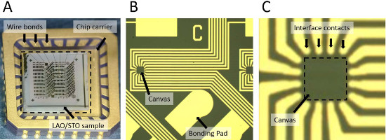
图2的光刻图案LAO / STO异质影像。(A)图片显示粘结到芯片载体5mm x 5mm的样品线(B)光学图像显示焊盘与画布之一。(C)特写一个单一的画布。 请点击此处查看该图的放大版本。

图3(A)非正式LAO / STO纳米结构的设计(B)纳米结构的采用开源的可伸缩矢量图形(SVG)的编辑器精确布局。

图4(A)平版印刷前面板为C-AFM图案(B)从截图3D仿真显示位置和C-AFM针尖电压。w.jove.com/files/ftp_upload/52058/52058fig4large.jpg"目标="_blank">请点击这里查看该图的放大版本。

图5(a)劳/ STO纳米结构被插入稀释制冷机(B)取样电阻的监测,因为它是从300K冷却到50 mK的。设备的四端微分电导(三)监测的一个函数侧栅极电压VSG和两端的电压装置(4T版)。西门子(S)为单位,并显示电压强度图显示在伏(V)为单位。
讨论
Successful creation of nanostructures depends on several critical steps. It is important that the LAO/STO samples are grown with a thickness that is known to be at the boundary between the insulating and conductive phase. (Details of sample growth fall outside the scope of this paper, but are crucial for overall success.) Second, it is important to have relative humidity within the range 25-45% for successful c-AFM writing. Values below 25% are unlikely to produce conductive nanostructures, while too high humidity will generally produce uncontrollably large features. Also, temperature control of the AFM is important if the c-AFM tip needs to achieve precise registry over long periods of time. Once the nanostructures are created, they must be placed in a vacuum environment if experiments lasting longer than a few hours are to be performed. For the experiments described here, the structure is created and within minutes transferred to a vacuum environment.
It is recommend before writing that a “writing test” be performed on all relevant electrodes. In such a test, two virtual electrodes are first created, and a single nanowire is written while simultaneously monitoring the conductance. A similar test of erasure can be performed by “cutting” the nanowire shortly afterwards. If the nanostructure is decaying rapidly, the issue is most likely due either to the interfacial contacts or the canvas itself. To distinguish between these two effects, a four-terminal measurement of the conductance should be performed, and the two-terminal conductance should be compared with the four-terminal conductance as a function of time. If the two-terminal conductance is decaying more rapidly than the four-terminal conductance, then the issue is related to the electrical contacts to the interface. If the four-terminal conductance is decaying at a comparable rate, then most likely the canvas is not suitable and should be replaced.
There are natural limitations of the current method for creating nanostructures. Specifically, the writing speed for the smallest devices is limited to a few hundred nanometers per second. Speeds far above that value lead to unpredictable results. Use of parallel writing techniques are possible27,28, but are not highly developed and have their own drawbacks. The size of nanostructures that can be created is naturally limited by the scan range of the AFM being used. A high-quality AFM with closed-loop feedback in the two scan directions is highly recommended. Tracking of point-like objects on the sample surface should be performed to monitor temporal drift of the sample.
Once creation of conductive nanostructures at oxide interfaces has been mastered, there are a wide range of experimental directions that can be explored. Using this technique, a wide variety of nanostructures and devices have already been demonstrated, including nanowires18, tunnel barriers29, rectifying junctions30, field-effect transistors18, single-electron transistors31, superconducting nanowires32, nanoscale optical detectors33, and nanoscale THz emitters and detectors34.
披露声明
The authors have nothing to disclose.
致谢
The long-standing collaboration with Chang-Beom Eom at the University of Wisconsin-Madison, who provided the LAO/STO samples, is gratefully acknowledged. Video editing assistance from Christopher Solis is greatly appreciated. This work is supported by NSF (DMR-1104191, DMR-1124131), ARO (W911NF-08-1-0317), and AFOSR (FA9550-10-1-0524, FA9550-12-1-0268, FA9550-12-1-0057).
材料
| Name | Company | Catalog Number | Comments |
| Equipment | |||
| Contact Aligner | Karl-Suss | MA6 | |
| Spinner | Solitec | 5110C | |
| Ion Mill | Commonwealth Scientific | 8C | |
| Sputtering System | Leybold-Heraeus | Z-650 | |
| Barrel Etcher | Branson/IPC | 3000C | |
| Wire Bonder | Westbond | 7700E | |
| AFM | Asylum Research | MFP-3D | |
| Dilution Refrigerator | Quantum Design | P850 | |
| Ultrasonic Wash Machine | Fisher Scientific | 15-335-6 | |
| Current Amplifier | Femto | DLPCA-200 | |
| Materials | |||
| LaAlO3/SrTiO3 | Prof. Chang-Beom Eom | 5 mm x 1 mm with ~3.4 unit cells of LAO (See Reference 18) | |
| Photoresist | AZ Electronic Materials | P4210 | |
| Developer | AZ Electronic Materials | 400K | |
| Acetone | Fisher Scientific | A929SK-4 | |
| Isopropyl Alcohol | Fisher Scientific | A459-1 | |
| Deionized Water | Fisher Scientific | 23-290-065 | |
| Gold Wire | DuPont | 5771 | 1 mm diameter |
| Chip Carrier | NTK Technologies | IRK28F1-5451D |
参考文献
- Sulpizio, J. A., Ilani, S., Irvin, P., Levy, J. i. . Annual Review of Materials Research, in press. , (2014).
- Mannhart, J., Blank, D. H. A., Hwang, H. Y., Millis, A. J., Triscone, J. M. Two-Dimensional Electron Gases at Oxide Interfaces. Mrs Bulletin. 33, 1027-1034 (2008).
- Zubko, P., Gariglio, S., Gabay, M., Ghosez, P., Triscone, J. -. M., Langer, J. S. Annual Review of Condensed Matter Physics. Interface Physics in Complex Oxide Heterostructures. , 141-165 (2011).
- Bogorin, D. F., Irvin, P., Cen, C., Levy, J. i., Tsymbal, E. Y., Dagotto, E. R. A., Chang-Beom, E., Ramesh, R. . Multifunctional Oxide Heterostructures. 13, (2012).
- Granozio, F. M., Koster, G., Rijnders, G. Functional Oxide Interfaces. MRS Bulletin. 38, 1017-1023 (2013).
- Ohtomo, A., Hwang, H. Y. A high-mobility electron gas at the LaAlO3/SrTiO3 heterointerface. Nature. 427, 423-426 (2004).
- Reyren, N., et al. Superconducting interfaces between insulating oxides. Science. 317, 1196-1199 (2007).
- Bark, C. W., et al. Switchable Induced Polarization in LaAlO3/SrTiO3 Heterostructures. Nano Letters. 12, 1765-1771 (2012).
- Brinkman, A., et al. Magnetic effects at the interface between non-magnetic oxides. Nature Materials. 6, 493-496 (2007).
- Thiel, S., Hammerl, G., Schmehl, A., Schneider, C. W., Mannhart, J. Tunable quasi-two-dimensional electron gases in oxide heterostructures. Science. 313, 1942-1945 (2006).
- Cen, C., et al. Nanoscale control of an interfacial metal-insulator transition at room temperature. Nature Materials. 7, 298-302 (2008).
- Singh-Bhalla, G., et al. Built-in and induced polarization across LaAlO3/SrTiO3 heterojunctions. Nature Physics. 7, 80-86 (2011).
- Li, L., et al. Very Large Capacitance Enhancement in a Two-Dimensional Electron System. Science. 332, 825-828 (2011).
- Xie, Y., Hikita, Y., Bell, C., Hwang, H. Y. Control of electronic conduction at an oxide heterointerface using surface polar adsorbates. Nature Communications. 2, 494 (2011).
- Bark, C. W., et al. Tailoring a two-dimensional electron gas at the LaAlO3/SrTiO3 (001) interface by epitaxial strain. PNAS. 108, 4720-4724 (2011).
- Tra, V. T., et al. . Adv Mater. 25, 3357-3364 (2013).
- Cronenwett, S. M., Oosterkamp, T. H., Kouwenhoven, L. P. A Tunable Kondo Effect in Quantum Dots. Science. 281, 540-544 (1998).
- Cen, C., Thiel, S., Mannhart, J., Levy, J. Oxide Nanoelectronics on Demand. Science. 323, 1026-1030 (2009).
- Kalinin, S. V., Gruverman, A. . Scanning probe microscopy: electrical and electromechanical phenomena at the nanoscale. 1, (2007).
- Piner, R. D., Zhu, J., Xu, F., Hong, S. H., Mirkin, C. A. 'Dip-pen' nanolithography. Science. 283, 661-663 (1999).
- Ahn, C. H., et al. Nonvolatile Electronic Writing of Epitaxial Pb(Zr0.52Ti0.48)O3/SrRuO3 Heterostructures. Science. 276, 1100-1103 (1997).
- Bi, F., et al. 'Water-cycle' mechanism for writing and erasing nanostructures at the LaAlO3/SrTiO3 interface. Applied Physics Letters. 97, 173110 (2010).
- Cheng, G., et al. Anomalous Transport in Sketched Nanostructures at the LaAlO3/SrTiO3 Interface. Phys Rev X. 3, 011021 (2013).
- Veazey, J. P., et al. Nonlocal current-voltage characteristics of gated superconducting sketched oxide nanostructures. Europhys Lett. 103, 57001 (2013).
- Veazey, J. P., et al. Oxide-based platform for reconfigurable superconducting nanoelectronics. Nanotechnology. 24, 375201 (2013).
- Irvin, P., et al. Anomalous High Mobility in LaAlO3/SrTiO3 Nanowires. Nano Letters. 13, 364-368 (2013).
- Salaita, K., et al. Massively Parallel Dip–Pen Nanolithography with 55 Two-Dimensional Arrays. Angewandte Chemie. 118, 7378-7381 (2006).
- Li, S., et al. Parallel Conductive-AFM Lithography on LaAlO3/SrTiO3 Interfaces. Ieee T Nanotechnol. 12, 518-520 (2013).
- Cen, C., Bogorin, D. F., Levy, J. Thermal activation and quantum field emission in a sketch-based oxide nanotransistor. Nanotechnology. 21, 475201 (2010).
- Bogorin, D. F., et al. Nanoscale rectification at the LaAlO3/SrTiO3 interface. Applied Physics Letters. 97, 013102 (2010).
- Cheng, G., et al. Sketched Oxide Single-Electron Transistor. Nature Nanotech. 6, 343-347 (2011).
- Joshua, A., Ruhman, J., Pecker, S., Altman, E., Ilani, S. Gate-tunable polarized phase of two-dimensional electrons at the LaAlO3/SrTiO3 interface. PNAS. 110, 9633 (2013).
- Irvin, P., et al. Rewritable Nanoscale Oxide Photodetector. Nature Photon. 4, 849-852 (2010).
- Ma, Y., et al. Broadband Terahertz Generation and Detection at 10 nm Scale. Nano Letters. 13, 2884-2888 (2013).
转载和许可
请求许可使用此 JoVE 文章的文本或图形
请求许可探索更多文章
This article has been published
Video Coming Soon
版权所属 © 2025 MyJoVE 公司版权所有,本公司不涉及任何医疗业务和医疗服务。