
Method Article
작성 및 산화물 나노 구조의 저온 특성
요약
Oxide nanostructures provide new opportunities for science and technology. The interfacial conductivity between LaAlO3 and SrTiO3 can be controlled with near-atomic precision using a conductive atomic force microscopy technique. The protocol for creating and measuring conductive nanostructures at LaAlO3/SrTiO3 interfaces is demonstrated.
초록
Oxide nanoelectronics is a rapidly growing field which seeks to develop novel materials with multifunctional behavior at nanoscale dimensions. Oxide interfaces exhibit a wide range of properties that can be controlled include conduction, piezoelectric behavior, ferromagnetism, superconductivity and nonlinear optical properties. Recently, methods for controlling these properties at extreme nanoscale dimensions have been discovered and developed. Here are described explicit step-by-step procedures for creating LaAlO3/SrTiO3 nanostructures using a reversible conductive atomic force microscopy technique. The processing steps for creating electrical contacts to the LaAlO3/SrTiO3 interface are first described. Conductive nanostructures are created by applying voltages to a conductive atomic force microscope tip and locally switching the LaAlO3/SrTiO3 interface to a conductive state. A versatile nanolithography toolkit has been developed expressly for the purpose of controlling the atomic force microscope (AFM) tip path and voltage. Then, these nanostructures are placed in a cryostat and transport measurements are performed. The procedures described here should be useful to others wishing to conduct research in oxide nanoelectronics.
서문
산화물 헤테로 1-5 전시 과학적으로 흥미로운 응용 프로그램 4 잠재적으로 유용한 응급 물리적 현상의 매우 다양한 종류. 특히, LaAlO3는 (LAO) 및 3 된 SrTiO3 (STO) (6) 사이의 인터페이스는 8 강유전체 조 및 강자성 구 동작 7 초전도, 전도성, 절연성을 나타낼 수있다. 2006 년 틸 등이 LAO 층의 두께와 같은 날카로운 절연체 - 금속 전이가 있음을 보여 주었다 (10)은 4 단위 셀 (4uc)의 임계 두께에 따라 증가한다. 그것은 이후 3uc-LAO/STO 구조가 전도성 원자 힘 현미경 (C-AFM) 탐침 (11)와 로컬로 제어 할 수있는 이력 전환을 나타내는 것으로 나타났다.
예컨대 LaAlO3는 / 3 된 SrTiO3 등의 산화물 인터페이스의 특성은 도전성의 부재 또는 존재에 의존계면에서 전자. 이 전자가 위로 게이트 전극 (12, 13), 게이트 (10)를 사용하여 제어 할 수 있습니다, 표면 (14) 흡착, 강유전체 층 (15, 16)과 C-AFM 리소그래피 11. C-AFM 리소그래피의 독특한 기능은 매우 작은 나노 기능을 생성 할 수 있다는 것입니다.
두 차원 감금과 함께 전기 톱 게이트는 종종 III-V 반도체 (17) 양자 도트를 만드는 데 사용됩니다. 대안 적으로, 준 일차원 반도체 나노 와이어는 전기적으로 근접하여 게이팅 될 수있다. 이러한 구조의 제조 방법은 시간 소모적이고, 일반적으로 비가 역적이다. 대조적으로, C-AFM 리소그래피 기술은 나노 구조물이 한 실험에 대해 생성 한 다음, (화이트 보드와 유사한) "소거"될 수 있다는 점에서 가역적이다. 삭제, 동안 일반적으로, C-AFM 쓰기는 AFM 팁에 적용 양의 전압으로 수행음의 전압을 사용하여 수행된다. 특정한 구조를 생성하는 데 필요한 시간은 디바이스의 복잡성에 의존하지만, 일반적으로 30 분 미만이고; 그 시간의 대부분은 캔버스를 삭제 소요됩니다. 일반적인 공간 해상도는 약 10 나노 미터입니다 만, 2 나노 미터 (18)를 생성 할 수있는 적절한 튜닝은 작은 있습니다.
나노 제조 절차의 상세한 설명은 다음과 같다. 여기에 제공된 내용은 비슷한 실험이 관심이 연구자에 의해 수행 될 수 있도록 충분해야한다. 여기에 설명 된 방법은 반도체에 전자 나노 구조를 만드는 데 사용되는 기존의 리소그래피 방법에 비해 많은 장점을 가지고 있습니다.
여기에 기재된 C-AFM 리소그래피 방법은 주사 양극 산화 (19), 딥 - 펜 나노 리소그래피 (20), 압전 패터닝 등 스캐닝 프로브 기반 리소그래피 노력의 훨씬 광범위한 클래스의 일부인21, 등등. 신규 산화물 인터페이스의 사용과 함께 여기에 설명 C-AFM 기술은, 물성의 전례 다양한 높은 정밀도의 전자 구조의 일부를 생성 할 수있다.
프로토콜
1. LAO / STO 헤테로를 얻
- 티오이 종료 STO 기판에 펄스 레이저 증착법에 의해 성장 LAO의 3.4 단위 전지로 구성된 산화물 헤테로 구조를 얻습니다. 샘플 성장의 세부 사항 참조. 22에 설명되어 있습니다.
샘플 2. 포토 리소그래피 처리
칩 캐리어에 배선 캔버스를위한 본딩 패드와 LAO / STO 인터페이스에 전기 접점을 만듭니다. 개별 처리 단계는 아래에 상세히 설명된다.
- 스핀 포토 레지스트
- 다음 30 초 동안 4,000 rpm에서 5 초 동안 600 rpm에서 샘플에 포토 레지스트를 스핀. 포토 레지스트 층은 약 2 μm의 두께 일 것이다. 1 분 동안 95 ° C에서 샘플을 굽는다.
- 5 mW의 / ㎠의 복용량 100 초 동안 320 nm의 빛을 마스크 얼 라이너를 사용하여 포토 레지스트를 노출합니다.
- fo를 포토 레지스트 개발에 포토 레지스트를 개발1 분 R.
- 이온 밀링
- 포토 레지스트에 포함되지 분야에서 15 소재의 뉴 멕시코 (LAO와 STO)를 제거하기 위해 아르곤 + 이온 밀을 사용합니다. 들어오는 아르곤 + 이온 빔에 수직 인 방향으로 22.5 ° 각도로 샘플을 놓습니다. 아르곤 + 에칭 속도가 보정되지 않은 경우, 재료의 정확한 양이 제거 될 수 있도록 교정 실행을 수행합니다. AFM 또는 이에 상응하는 profilmetry를 사용하여 식각 깊이를 결정합니다.
- TI와 금의 DC 스퍼터링
- 입금 4 nm의 TI는 다음의 Au 노출 STO 층과 전기적으로 접촉을 시료 위에 25 nm의 금하게되도록. 스퍼터링 압력 범위 2-6 X 10⁻⁷ 토르이며, 스퍼터링은 RT에서 샘플로 이루어진다. TI는 셔터와 함께 10 분 동안 열린 셔터 후, 100 W로 마감 전 스퍼터 완료되면 100 W.에서 20 초 동안 스퍼터, 바로 50 W에서 1 분 동안 금을 미리 스퍼터 다음에 샘플을 30 초 동안 금을 스퍼터 50 W. 칼리소망의 Ti와 두께의 Au를 생성하는 시간을 브레이트.
- 이륙
- 샘플의 표면에서 포토 레지스트를 제거하기 위해 아세톤 / IPA 초음파 세척을 사용합니다.
- 두 번째 층
- 4 단계 (예. 제외 이온 밀링)을 제외하고 두 번째 리소그래피 공정은, 각각의 본딩 패드에 골드 와이어 연결을 작성하는 데 사용됩니다. 두 가지 패턴들은 전기 단락을 생성하지 않도록 잘 정렬되어야합니다.
- 플라즈마 세정.
- IPC 배럴 에처는 트렌치 패턴에 포토 레지스트 잔류 물을 제거하기 위해 사용된다. 1 분 동안 100 W, 1 Torr의 아르곤에서 사용 계측기
3. 와이어 본드 샘플 쓰기를 준비하는
- 28 사용 가능한 핀 칩 캐리어 (그림 2A)에 LAO / STO 샘플을 장착합니다.
- 와이어 결합 구조
참고 : 전기 C를 만들기 위해 와이어 본더를 사용샘플에 본딩 패드와 칩 캐리어 사이 onnections. 전기 접점 및 칩 캐리어 사이에 1 밀 (25 마이크로 미터) 골드 와이어를 연결합니다. 나노 쓰기
4. 나노 구조를 쓰기
- 전도성 나노 구조 (그림 3A)의 비공식 스케치를 만듭니다.
- 확장 가능한 벡터 그래픽 (SVG) 편집기 (그림 3B)를 엽니 다.
- 템플릿을 사용하거나 AFM 이미지의 일치하도록 창 크기를 정의합니다.
- SVG 편집기에 시료의 AFM 이미지를로드합니다.
- AFM 이미지에 중첩 나노 구조 요소를 만듭니다.
- 나노 리소그래피 프로그램에 SVG 파일을로드합니다.
- 전도성 나노 구조를 만들 수 리소그래피 소프트웨어를 실행합니다.
- 사용 V 팁 = +10 나노 구조를 만들 수있는 V 및 V 팁 = 나노 구조를 지울 -10 V.
- 범위의 속도로 C-AFM 팁을 이동 202 μM / 초의 0 ㎚ / 초.
5. 장치를 냉각 및 측정을 수행
- 모두 흰색 조명을 끄고 빨간색 필터 / 라이트 소스를 사용합니다.
- AFM 시스템에서 샘플을 추출합니다.
- 희석 냉장고 (A)에 샘플을로드합니다.
- 샘플이 냉각으로 온도 (B) 대 저항을 측정합니다.
- 낮은 온도 (C)에 전송 특성을 측정한다.
결과
결과는 여기에 도시 된 나노 구조물이 클래스에 의해 발휘된다 반송 동작을 대표하며 그 밖에 23-26 상세히 설명되었다. 이 예에서, 나노 와이어 캐비티는 3.3 단위 셀 LAO / STO 헤테로 구조에서 (도 4)를 구성하고있다. 실험 11 "절단"나노 와이어에 의해 결정 (녹색으로 표시) 도전은 넓은 일반적으로 10 ㎚이다. 팁 쓰기 속도는 각 세그먼트의 끝 속도와 전압, 리소그래피 전면 패널 (그림 4B)에서 독립적으로 구성 할 수 있습니다. "가상 전극는"계면 연락처와 해당 인터페이스는 나노 구조에 전도성이 높은 전기 연결이 있는지 확인합니다.
나노 구조가 기록 된 후에는 희석 냉동기로 전달된다. 550 나노 미터 이하에서 빛에 대한 노출은 원치 않는 광전도를 생성합니다, 그래서 꼬마 도깨비ortant 어둠 또는 빨간색 "암실"빛 (그림 5A)의 도움으로 장치를 전송합니다. 전기 연결은 RT에서 수행되어야하고, 극저온에서 전기 연결을 변경할 때 대부분의 반도체 나노 구조와 같은 큰주의를 기울여야합니다. 장치가 정전기 방전을 실시하면, 가장 가능성이 절연 될 것이다. 현저하게, 디바이스 기능은 "순환"300 K까지 온도를 다시 냉각하여 회수 할 수있다.
쿨 다운 동안, 2 단자의 저항을 모니터링하는 루틴, 심지어 4 단자 저항, 온도의 함수로서. AC 전류는 트랜스 임피던스 증폭기를 사용하여 측정되는 동안 이러한 측정을 위해 AC 전압 (일반적으로 1 ~ MV)는, 전극들 중 하나에 저주파 (<10 헤르쯔)에인가된다. 복조 잠금 및 필터링은 집에서 개발 한 잠금 앰프를 사용하여 수행됩니다. 교류 세제곱rrent는 온도의 함수 (그림 5B)로 감시된다.
장치가 희석 냉장고 (50 mK의)의베이스 온도로 냉각되면, 4 단자 전송 측정 (도 5c)이 수행된다. 장치를 통해 전압을 동시에 측정하는 동안 이러한 측정의 경우, 현재는 장치의 기본 채널을 통해 공급된다. 대신 잠금 앰프, 전체 전류 - 전압 측정의 (IV) 추적을 측정한다. 이 방법은 더 많은 정보를 포함하고 차동 도통 수치 분화를 통해 계산 될 수있다. 특정 장치, 차동 도통 사이드 게이트 전압 V에 SG의 함수로서 측정된다. 이 게이트 디바이스의 화학 전위가 변화 될 수있다. 장치를 통해 전송은 쿨롱 봉쇄 작은 값을 발생하고, 스트로크 엔진을하는 영역을 나타내는 강력한 단순하지 않은 의존성을 보여줍니다V의 SG의 큰 값을 초전도 겨. 장치의이 클래스에 대한 물리적 해석에 대한 자세한 내용은 다른 곳에서 설명한다.

..도 1 포토 리소그래피 공정 단계 단계 1 : 스핀 포토 레지스트. 2 단계 : 마스크 얼 라이너를 사용하여 포토 레지스트를 노출합니다. 3 단계 : 포토 레지스트를 개발한다. 4 단계 : 이온 밀링. 5 단계 : DC는 티타늄과 금을 증착하는 스퍼터링. 6 단계 : 리프트 오프 (lift-off). 7 단계 : 두 번째 층을 증착. 8 단계 : 플라즈마 세정.

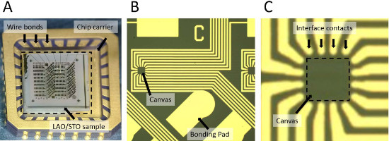
그림 2. 리소그래피 패터닝 LAO / STO 헤테로의 이미지. 칩 캐리어에 결합는 5mm X 5mm는 샘플 와이어를 보여주는 (A) 이미지. (B) 본딩 패드와 캔버스 중 하나를 보여주는 광학 이미지. (C) 하나의 캔버스의 근접입니다. 이 그림의 더 큰 버전을 보려면 여기를 클릭하십시오.

그림 3. LAO / STO 나노 구조의 (A) 비공식 디자인. (B) 오픈 소스 확장 가능한 벡터 그래픽 (SVG) 편집기를 사용하여 나노 구조의 정확한 레이아웃입니다.

그림 4. C-AFM의 패터닝 (A) 리소그래피 전면 패널. (B) 3 차원 시뮬레이터의 스크린 샷 위치와 C-AFM 팁의 전압을 표시합니다.w.jove.com/files/ftp_upload/52058/52058fig4large.jpg "대상 ="_blank ">이 그림의 더 큰 버전을 보려면 여기를 클릭하십시오.

도 5. (A) LAO / STO 나노 구조물이 희석 냉동기에 삽입된다. (B) 시료의 저항의 모니터링이 50 mK의 300 내지 K로부터 냉각 될 때. 장치의 4 단자 차분 컨덕턴스 (C) 모니터링의 함수 장치 (V4t)에서 사이드 게이트 전압를 Vsg 전압. 지멘스 (S)의 단위 및 전압에 표시 강도 그래프는 볼트 (V) 단위로 표시됩니다.
토론
Successful creation of nanostructures depends on several critical steps. It is important that the LAO/STO samples are grown with a thickness that is known to be at the boundary between the insulating and conductive phase. (Details of sample growth fall outside the scope of this paper, but are crucial for overall success.) Second, it is important to have relative humidity within the range 25-45% for successful c-AFM writing. Values below 25% are unlikely to produce conductive nanostructures, while too high humidity will generally produce uncontrollably large features. Also, temperature control of the AFM is important if the c-AFM tip needs to achieve precise registry over long periods of time. Once the nanostructures are created, they must be placed in a vacuum environment if experiments lasting longer than a few hours are to be performed. For the experiments described here, the structure is created and within minutes transferred to a vacuum environment.
It is recommend before writing that a “writing test” be performed on all relevant electrodes. In such a test, two virtual electrodes are first created, and a single nanowire is written while simultaneously monitoring the conductance. A similar test of erasure can be performed by “cutting” the nanowire shortly afterwards. If the nanostructure is decaying rapidly, the issue is most likely due either to the interfacial contacts or the canvas itself. To distinguish between these two effects, a four-terminal measurement of the conductance should be performed, and the two-terminal conductance should be compared with the four-terminal conductance as a function of time. If the two-terminal conductance is decaying more rapidly than the four-terminal conductance, then the issue is related to the electrical contacts to the interface. If the four-terminal conductance is decaying at a comparable rate, then most likely the canvas is not suitable and should be replaced.
There are natural limitations of the current method for creating nanostructures. Specifically, the writing speed for the smallest devices is limited to a few hundred nanometers per second. Speeds far above that value lead to unpredictable results. Use of parallel writing techniques are possible27,28, but are not highly developed and have their own drawbacks. The size of nanostructures that can be created is naturally limited by the scan range of the AFM being used. A high-quality AFM with closed-loop feedback in the two scan directions is highly recommended. Tracking of point-like objects on the sample surface should be performed to monitor temporal drift of the sample.
Once creation of conductive nanostructures at oxide interfaces has been mastered, there are a wide range of experimental directions that can be explored. Using this technique, a wide variety of nanostructures and devices have already been demonstrated, including nanowires18, tunnel barriers29, rectifying junctions30, field-effect transistors18, single-electron transistors31, superconducting nanowires32, nanoscale optical detectors33, and nanoscale THz emitters and detectors34.
공개
The authors have nothing to disclose.
감사의 말
The long-standing collaboration with Chang-Beom Eom at the University of Wisconsin-Madison, who provided the LAO/STO samples, is gratefully acknowledged. Video editing assistance from Christopher Solis is greatly appreciated. This work is supported by NSF (DMR-1104191, DMR-1124131), ARO (W911NF-08-1-0317), and AFOSR (FA9550-10-1-0524, FA9550-12-1-0268, FA9550-12-1-0057).
자료
| Name | Company | Catalog Number | Comments |
| Equipment | |||
| Contact Aligner | Karl-Suss | MA6 | |
| Spinner | Solitec | 5110C | |
| Ion Mill | Commonwealth Scientific | 8C | |
| Sputtering System | Leybold-Heraeus | Z-650 | |
| Barrel Etcher | Branson/IPC | 3000C | |
| Wire Bonder | Westbond | 7700E | |
| AFM | Asylum Research | MFP-3D | |
| Dilution Refrigerator | Quantum Design | P850 | |
| Ultrasonic Wash Machine | Fisher Scientific | 15-335-6 | |
| Current Amplifier | Femto | DLPCA-200 | |
| Materials | |||
| LaAlO3/SrTiO3 | Prof. Chang-Beom Eom | 5 mm x 1 mm with ~3.4 unit cells of LAO (See Reference 18) | |
| Photoresist | AZ Electronic Materials | P4210 | |
| Developer | AZ Electronic Materials | 400K | |
| Acetone | Fisher Scientific | A929SK-4 | |
| Isopropyl Alcohol | Fisher Scientific | A459-1 | |
| Deionized Water | Fisher Scientific | 23-290-065 | |
| Gold Wire | DuPont | 5771 | 1 mm diameter |
| Chip Carrier | NTK Technologies | IRK28F1-5451D |
참고문헌
- Sulpizio, J. A., Ilani, S., Irvin, P., Levy, J. i. . Annual Review of Materials Research, in press. , (2014).
- Mannhart, J., Blank, D. H. A., Hwang, H. Y., Millis, A. J., Triscone, J. M. Two-Dimensional Electron Gases at Oxide Interfaces. Mrs Bulletin. 33, 1027-1034 (2008).
- Zubko, P., Gariglio, S., Gabay, M., Ghosez, P., Triscone, J. -. M., Langer, J. S. Annual Review of Condensed Matter Physics. Interface Physics in Complex Oxide Heterostructures. , 141-165 (2011).
- Bogorin, D. F., Irvin, P., Cen, C., Levy, J. i., Tsymbal, E. Y., Dagotto, E. R. A., Chang-Beom, E., Ramesh, R. . Multifunctional Oxide Heterostructures. 13, (2012).
- Granozio, F. M., Koster, G., Rijnders, G. Functional Oxide Interfaces. MRS Bulletin. 38, 1017-1023 (2013).
- Ohtomo, A., Hwang, H. Y. A high-mobility electron gas at the LaAlO3/SrTiO3 heterointerface. Nature. 427, 423-426 (2004).
- Reyren, N., et al. Superconducting interfaces between insulating oxides. Science. 317, 1196-1199 (2007).
- Bark, C. W., et al. Switchable Induced Polarization in LaAlO3/SrTiO3 Heterostructures. Nano Letters. 12, 1765-1771 (2012).
- Brinkman, A., et al. Magnetic effects at the interface between non-magnetic oxides. Nature Materials. 6, 493-496 (2007).
- Thiel, S., Hammerl, G., Schmehl, A., Schneider, C. W., Mannhart, J. Tunable quasi-two-dimensional electron gases in oxide heterostructures. Science. 313, 1942-1945 (2006).
- Cen, C., et al. Nanoscale control of an interfacial metal-insulator transition at room temperature. Nature Materials. 7, 298-302 (2008).
- Singh-Bhalla, G., et al. Built-in and induced polarization across LaAlO3/SrTiO3 heterojunctions. Nature Physics. 7, 80-86 (2011).
- Li, L., et al. Very Large Capacitance Enhancement in a Two-Dimensional Electron System. Science. 332, 825-828 (2011).
- Xie, Y., Hikita, Y., Bell, C., Hwang, H. Y. Control of electronic conduction at an oxide heterointerface using surface polar adsorbates. Nature Communications. 2, 494 (2011).
- Bark, C. W., et al. Tailoring a two-dimensional electron gas at the LaAlO3/SrTiO3 (001) interface by epitaxial strain. PNAS. 108, 4720-4724 (2011).
- Tra, V. T., et al. . Adv Mater. 25, 3357-3364 (2013).
- Cronenwett, S. M., Oosterkamp, T. H., Kouwenhoven, L. P. A Tunable Kondo Effect in Quantum Dots. Science. 281, 540-544 (1998).
- Cen, C., Thiel, S., Mannhart, J., Levy, J. Oxide Nanoelectronics on Demand. Science. 323, 1026-1030 (2009).
- Kalinin, S. V., Gruverman, A. . Scanning probe microscopy: electrical and electromechanical phenomena at the nanoscale. 1, (2007).
- Piner, R. D., Zhu, J., Xu, F., Hong, S. H., Mirkin, C. A. 'Dip-pen' nanolithography. Science. 283, 661-663 (1999).
- Ahn, C. H., et al. Nonvolatile Electronic Writing of Epitaxial Pb(Zr0.52Ti0.48)O3/SrRuO3 Heterostructures. Science. 276, 1100-1103 (1997).
- Bi, F., et al. 'Water-cycle' mechanism for writing and erasing nanostructures at the LaAlO3/SrTiO3 interface. Applied Physics Letters. 97, 173110 (2010).
- Cheng, G., et al. Anomalous Transport in Sketched Nanostructures at the LaAlO3/SrTiO3 Interface. Phys Rev X. 3, 011021 (2013).
- Veazey, J. P., et al. Nonlocal current-voltage characteristics of gated superconducting sketched oxide nanostructures. Europhys Lett. 103, 57001 (2013).
- Veazey, J. P., et al. Oxide-based platform for reconfigurable superconducting nanoelectronics. Nanotechnology. 24, 375201 (2013).
- Irvin, P., et al. Anomalous High Mobility in LaAlO3/SrTiO3 Nanowires. Nano Letters. 13, 364-368 (2013).
- Salaita, K., et al. Massively Parallel Dip–Pen Nanolithography with 55 Two-Dimensional Arrays. Angewandte Chemie. 118, 7378-7381 (2006).
- Li, S., et al. Parallel Conductive-AFM Lithography on LaAlO3/SrTiO3 Interfaces. Ieee T Nanotechnol. 12, 518-520 (2013).
- Cen, C., Bogorin, D. F., Levy, J. Thermal activation and quantum field emission in a sketch-based oxide nanotransistor. Nanotechnology. 21, 475201 (2010).
- Bogorin, D. F., et al. Nanoscale rectification at the LaAlO3/SrTiO3 interface. Applied Physics Letters. 97, 013102 (2010).
- Cheng, G., et al. Sketched Oxide Single-Electron Transistor. Nature Nanotech. 6, 343-347 (2011).
- Joshua, A., Ruhman, J., Pecker, S., Altman, E., Ilani, S. Gate-tunable polarized phase of two-dimensional electrons at the LaAlO3/SrTiO3 interface. PNAS. 110, 9633 (2013).
- Irvin, P., et al. Rewritable Nanoscale Oxide Photodetector. Nature Photon. 4, 849-852 (2010).
- Ma, Y., et al. Broadband Terahertz Generation and Detection at 10 nm Scale. Nano Letters. 13, 2884-2888 (2013).
재인쇄 및 허가
JoVE'article의 텍스트 или 그림을 다시 사용하시려면 허가 살펴보기
허가 살펴보기더 많은 기사 탐색
This article has been published
Video Coming Soon
Copyright © 2025 MyJoVE Corporation. 판권 소유