Method Article
微流控气动笼:在芯片水晶捕获,处理的新方法和控制化学处理
摘要
Herein, we describe the fabrication and operation of a double-layer microfluidic system made of polydimethylsiloxane (PDMS). We demonstrate the potential of this device for trapping, directing the coordination pathway of a crystalline molecular material and controlling chemical reactions onto on-chip trapped structures.
摘要
The precise localization and controlled chemical treatment of structures on a surface are significant challenges for common laboratory technologies. Herein, we introduce a microfluidic-based technology, employing a double-layer microfluidic device, which can trap and localize in situ and ex situ synthesized structures on microfluidic channel surfaces. Crucially, we show how such a device can be used to conduct controlled chemical reactions onto on-chip trapped structures and we demonstrate how the synthetic pathway of a crystalline molecular material and its positioning inside a microfluidic channel can be precisely modified with this technology. This approach provides new opportunities for the controlled assembly of structures on surface and for their subsequent treatment.
引言
分子材料长期被研究在科学界,因为在诸如分子电子学,光学和传感器1-4他们的应用广泛的数目。在这些有机导体是一个特别令人兴奋的类,因为它们在柔性显示器和集成功能元件5,6的中心作用的分子的材料。然而,用于使能在基于分子的材料的电子电荷传输方法被限制的电荷输送配合物(的CTC)和电荷输送的盐(CTS消息)7-10的形成。频繁,的CTC和CTS消息是通过电化学方法或通过直接化学氧化还原反应产生的;妨碍供体或受体部分的受控转换到更复杂的结构,其中多功能可以设想流程。因此,为可控生成和分子基的操纵新系统的方法的澄清拆建物料仍保留在材料科学和分子工程领域的一个显著的挑战,如果成功,无疑将导致新的功能和新技术应用。
在这种情况下,微流体技术最近已用于合成基于分子的材料,由于其在合成过程11,12,以控制热与质量传递以及试剂的反应扩散体积的能力。简单地说,在连续的流动和在低雷诺数两个或更多个试剂流之间的稳定的接口,可以实现,其中,得到流路,其中,混合仅通过扩散13-16发生内部良好控制的反应区的形成。事实上,我们先前采用层流来本地化结晶分子材料,例如微流体通道17内的配位聚合物(CPS)的合成途径。虽然这种方法已经显示摹原位 18来实现在实现新颖的CP的纳米结构,所述直接集成这样的结构在表面上,以及控制化学处理它们的形成还没有经过REAT承诺。为了克服这一限制,最近我们表明,在两层微流体装置引入微流体气动笼(或阀门)的致动可以有利在这方面可以使用。由于地震的研究小组19的创举,微流控气动阀经常被用于单细胞捕获和隔离20,酶活性调查21,小的流体体积22俘获,在表面23和蛋白质结晶24功能材料的国产化。然而,我们已经表明,双层的微流体装置可用于捕获,本地化和原位整合形成的结构,以读出的组件和表面上的18。此外,我们还证明,这种技术可以用来在捕获结构进行控制的化学处理,使这两个"微流体辅助配体交换"18和控制的化学有机晶体18,25的掺杂。在这两种情况下,的CTC可以控制微流体的条件下进行合成,并在最近的研究中,多功能可以在相同的材料片进行说明。这里,我们证明采用染料载货流动这些双层的微流体装置的性能,产生和控制一个CP的协调通路以及其微流体通道的表面上的定位和最后评估控制的化学处理到芯片上被困结构。
研究方案
注意:一双层的微流体装置的两个层是使用一个绘图软件设计, 例如 ,AutoCAD和印刷,以形成高分辨率膜掩模,用5微米的特征精度的限制。主模具由SU-8光刻在4"硅晶片中创建,允许生产结构50微米的高度。
1.主模具制造使用SU-8光刻
- 放置在硅晶片上的热板上10分钟来脱水设定在200℃。
注:硅晶片脱水提供了更好的接触,并确保对SU-8光致抗蚀剂的旋涂步骤中的扩频。 - 冷却该脱水晶片至室温历时3分钟。
- 装载在晶片上旋转涂布机和存款4毫升的SU-8光致抗蚀剂中的晶片的中心(约1毫升的SU-8每衬底英寸)。
- 首先,传播沉积SU-8慢慢在500 revoluti每分钟(rpm)组件10秒。这样的旋转速度,确保的SU-8的覆盖在整个晶片表面增加。
- 其次,通过以更高的速度旋转该衬底控制的SU-8的厚度。在目前的实验中,使用3000rpm的旋转速度为30秒,以产生的SU-8设有50微米高。
- 擦拭晶片同时以低转速(通常为100转)旋转小心用棉擦拭的边珠。
- 在95℃下加热的热板上的旋涂的晶片15分钟,从SU-8( 即 ,"软烘烤")除去残留的溶剂。
注意:模式或"皱纹",在抗蚀剂层的存在指示该不完全除去溶剂。 - 冷却该焙烧晶片回落到室温,并在光掩模的乳剂打印面与前曝光晶片接触。
- 打开紫外灯和曝光单元上,并让系统稳定一段10米英寸(根据时间=曝光能量/在365nm强度)测量灯强度在365nm用紫外视力计,并估计所需的曝光时间。
注意:在当前实验中的曝光能量计算为250毫焦/厘米2。 - 露出旋涂的晶片于UV光在先前步骤中所估计的时间上的光掩模。在这里,揭露了79.6秒。
- 曝光后立即烘烤的热板上曝光晶片在65℃下1分钟,随后在95℃下5分钟。在该步骤中,反应通过UV -light发起和烘烤后完成。
- 离开后烘烤晶片历时3分钟冷却至室温。
- 通过在8分钟在SU-8显影剂溶解它开发非交联SU-8在晶片上。为了确保能完全消除非交联SU-8的,分裂过程分为两个步骤。
- 在第一,沉浸在显影剂溶液中的晶片5分钟,再移动的大多数非交联SU-8。
- 然后浸泡在显影剂的新鲜溶液晶片3分钟以溶解剩余的非交联SU-8(通常受困交联结构之间)。
- 冲洗显影晶片用异丙醇,并让具有图案化结构中的晶片(以下简称为"母模")站干。漂洗后的母模乳白色的残留物的观察表明,发展是不完整的。
- 加热的热板上干燥母模在200℃下2-5分钟,以"硬烘焙"中的抗蚀基板和退火潜在的裂纹。
- 允许所制造的母模冷却至室温。
- 放置在通风橱内,在干燥器的母模(连接到一个真空泵)。
- 倾100μl的三甲基氯硅烷(TMCS)到玻璃烧杯中,并把这个干燥器内。
注意:TMCS是易燃,corrosive和毒性;因此,处理步骤应在通风橱内进行,与戴防护手套,护目镜和白大褂的用户。 - 把干燥器真空并等待至少1小时,让TMCS蒸气沉积在母模的表面。
- 1小时后,慢慢地平衡干燥器内并到大气中的压力打开。
注意:不要直接开干燥器上述呼吸。 - 取出硅烷化主机和关闭干燥器。
2.双层微流体装置的研制
注意:该协议是对时间和温度特别敏感。任何不遵循的时间帧和温度可能会导致非粘合的,因此,非功能器件的制造。
- 倾PDMS弹性体和固化剂的混合物,(5:1的重量比)到一次性称量皿,并用塑料刮铲充分混合。在目前的实验S,使用50克弹性体和10克固化剂,以形成一个PDMS层约5mm的高度19,26。
- 放置均匀混合的PDMS在真空下干燥器中脱气和除去夹带的气泡为15分钟。
- 混合的PDMS弹性体和固化剂(20:1的重量比)在一次性称量盘( 例如 ,10g的弹性体和0.5克固化剂)19,26。
- 修复一帧中的"控制层"母模(在当前的实验中,一个11毫米的圆形聚四氟乙烯(PTFE)环)。
- 15分钟后,放置20:在干燥器1的PDMS混合物在真空下脱气。
- 从干燥器1 PDMS的混合物倒到这是位于圆框里面的"控制层"母模:在同一时间,前面的步骤,取出5。放置装有与PDMS和母模进入在真空下的干燥器以及该帧。保持顺差PDMS。
- 45分钟后(30分钟后推ING都PDMS混合物放入干燥器),取两者PDMS混合物出干燥器,并放置含5帧:1 PDMS和在80℃的"控制层"模具师傅在烤箱。
- 与此同时,开始旋涂的"流体层"母模与20:1混合PDMS。用于旋涂的旋转速度根据所需的高度来确定,并且已在别处27日报道。瞄准60分钟以终止旋涂,并保持剩余的PDMS。
- 60分钟后,把涂覆有20"流体层"母模旋:1的PDMS入烘箱中在80℃。
- 在75分钟,取这两个主模具出炉。
- 剥离只有5:从"控制层"母模1 PDMS,骰子用刀片基体,并在设计中确定的入口位置1毫米的穿刺活检冲床冲床控制层的孔中。这里,控制层是在长度为24毫米和为24mm宽度。
- - [R从使用胶带切割好的芯片emove碎屑。
- 手动组装切块并在20的顶部穿孔控制层芯片:涂覆在使用具有500X的放大倍数在立体显微镜( 图1)中的"流体层"母模1的PDMS自旋。
- 倒入周围画组装芯片的残余PDMS,使较厚的PDMS层,从而有利于在年底拆除保税流体和控制层。
- 放置装有在烘箱两个层设备的"流体层的"主模在80℃和储存过夜。
- 第二天,取该固化组件出炉并使其冷却至室温。
- 剥离从"流体层"母模与PDMS组件,骰子用刀片的制造的双层器件(24毫米长和24毫米宽)和冲头的流体入口/出口用1.5毫米的活检穿孔。
- 对待与OPE芯片表面n个信道和盖玻片(24毫米×40毫米),电晕放电,并立即粘结在一起。超过1分钟移动在PDMS板和玻璃盖玻片电晕放电处理。另外,使用台式等离子系统,以方便粘合。
- 在70-80℃下储存在烘箱粘合双层芯片至少4小时。
3.微流控系统组装
- 微流体装置已被组装之后,用聚四氟乙烯(PTFE)管(1.3毫米内径)芯片的流体层的入口连接到流体储(注射器)。
- 连接压力供给源,使用硅橡胶管和金属连接器具有1.6毫米的外径控制层入口。
- 打开和使用由手动操作的压力源在3巴施加加压空气关闭阀门。使用一系列计算机控制的注射泵的供给流体通道。
- 可视化的阀门驱动和设备操作与安装在倒置显微镜高分辨率摄像头。使用5X到63X的放大倍率。
4.操作层流状态由气动执行机构凯奇
注意:流体层包括两个入口会聚通道,其在宽度150微米,更广泛的主通道300微米的宽度。并且控制层具有一系列位于主流体通道的顶端相同的长方形阀(250微米×200微米)。
- 一旦设定了连接到注射器泵和气动控制器的系统,通过以20微升/分钟的流速在入口通道中的一个引入含水染料流。
- 通过在3巴驱动它关闭阀门。
- 请注意,流体仍然可以流阀周围。此功能是实现控制化学处理被困结构18,25的重要</ SUP>。
- 通过释放压力打开阀门。
- 而将染料溶液流过第一通道,注入另一种水性流体送入第二进口通道20微升/分钟。两种水溶液流之间的界面是由于存在于微流体设备中的层流状态形成。
- 通过在3巴驱动它关闭阀门。在这种情况下,阀的致动改变了两种水溶液流的接口;可用于在CP( 参见下文 )18,28的形成过程中修改合成途径的结果。
- 改变流体流速至30微升/分钟,10微升/分钟,并观察向下或向上移引导两种流体之间产生界面。
5.本地化的微粒
- 连接所制造的双层芯片到注射器泵和气动控制器的系统。
- 制备含有10%(重量)的聚苯乙烯的水溶液荧光体颗粒(分别为5微米的直径,激发和发射最大值在468纳米和508纳米)。
- 使用在488纳米的波长下操作激光激发源。
- 引入含颗粒的流体进入两个进入通道以20微升/分钟的总流速。
- 等待2分钟,直到稳定的流被建立。
- 将阀门在3巴将其关闭。几个颗粒将被夹在阀的下面,并同时将流保持在表面上的局部。
6.生成和配位聚合物的可控的降低(CP)
- 制备硝酸银的2.5 mM溶液( 硝酸银)。
- 准备半胱氨酸(半胱氨酸)为2.5 mm的水溶液。
- 制备在乙醇18的饱和抗坏血酸溶液。
- 使用相同的双层芯片和两种试剂注入到两个进入通道(每个入口一种试剂)的每个以流速50微升/分钟。
- 观察两个共同流入水蒸气的界面银和半胱氨酸(银(Ⅰ)的Cys)CP的形成。
- 将阀门在3巴套住形成的Ag(I)半胱氨酸的CP阀下方。
- 冲洗蒸馏水成以50μl的流速的入口通道/分钟洗去在合成过程中使用的过剩的试剂。
- 释放压力并打开阀门。所生成的CP的保持停流条件下的阀的下方。
- 为了进行受控化学还原捕集的Ag(I)的半胱氨酸的CP时,释放阀压力在1巴,并以10微升/分钟的流速冲洗的乙醇饱和抗坏血酸溶液。
- 观察到归因于((0)的Ag)由抗坏血酸18还原银(Ⅰ)为金属银的清楚的颜色变化。
结果
双层微流体装置包括在PDMS结构粘结的微流控芯片, 如图1。第一层,它是在键合到表面的同时,被用于流动流体(液体层),而第二层,这是直接键合到第一PDMS层,用于流气体(控制层)。

图1.双层微流体装置。(A)示意图,并在我们的调查中使用的双层微流体装置( 二 )显微照片。 请点击此处查看该图的放大版本。
通过在通道的气体的注射控制层挤压朝向表面( 图2A和图2B)中的流体层,允许结构的捕集和本地化微流体通道表面上。 PDMS膜致动可以用来产生气动笼和/或由一个气动控制器控制微阀。作为膜致动的范例模型中,我们表明,流体层的完整偏转如何避免了染料的载货流分发其致动( 图2C)和微通道表面上的荧光微粒的捕集后的阀下方( 图2D和2E) 。

图2.膜驱动和诱捕结构。(A)侧和(B)顶视图插图显示双层微流体装置是前(上)和后气动阀的(底部)致动。双层的微流体装置(C)的显微照片之前(上图)和流体层(底部)的挤压后。在底部面板,流体层填充有若丹明染料的膜致动的一个更好的感知的水溶液。 (D)的前(顶)双层的微流体装置的明视场显微照片和后(底)用流动的水溶液含有溶液的聚苯乙烯荧光发色粒子在阀的致动(10重量%)。在D所示的光学显微镜图像(E)荧光图像请点击此处查看该图的放大版本。
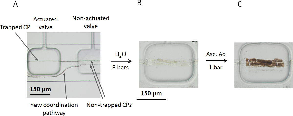
图3A示出的原位捕获生成的CP的双层微流体装置内部通过actuat气动笼离子。请注意,一个新的协调通路的第一阀的致动之后产生。阀致动确保了银(Ⅰ)的Cys在两个试剂流的界面产生CP的俘获并促进新的协调通路( 图3A)的形成。银(I)半胱氨酸的两个试剂流的界面产生CP的详细化学特性可以在以往的研究17,18找到。此外,与后除去多余的试剂溶液用纯水( 图3B)的流动,在乙醇中的饱和抗坏血酸溶液可以添加到用于受控化学还原芯片上捕获结构( 图3C)的微流体通道。减少3个酒吧,以1杆阀门压力有利于被困银(I)半胱氨酸CP夹紧区18下方的控制化学处理。被困银(I)半胱氨酸CP的颜色变化至黑褐色是ttributed到一价银的还原到金属,在符合以前的观察18,29。

图3.陷印银(I)半胱氨酸CP和控制化学还原法。(A)光学显微镜图像显示的原位原料合成一个新的协调途径的银(I)半胱氨酸CP和产生诱捕。钳位区域下面困的CP(二)显微照片水流去除多余的试剂的解决方案后,并在(C),还原反应过程后,同样的微阀的显微照片。 请点击此处查看大图这个数字。
讨论
The reported approach can be easily modified to fabricate different valve shapes to afford other applications such as fluid confinement. Indeed, the flexibility of this protocol also allows for modification of the thickness of the bottom layer, and thereby of the PDMS membrane, from a couple of tens to a few hundreds of microns to fulfill any application of interest. Moreover, dimensions of structures in each layer of the device can be optimized for the desired application and various heights of structures on the master molds can be simply achieved by spinning the photoresist at different velocities. Spinning the photoresist at a higher speed results in thinner structures.
To better implement the protocol, a clean room environment for the fabrication of the master molds is substantially essential; otherwise, the fabrication procedure will lead to defective master molds and thereby to unusable microfluidic devices. Two critical aspects should be emphasized in this protocol: i) the constant temperature of the oven that needs to be adjusted to 80 °C and ii) the programmed time period between processes that has to be complied accurately. Any modification of temperature and time frame in the protocol might lead to non-bonded chips, and thus, to non-functional devices.
The "turbulent free" conditions typically encountered in microfluidic systems have recently been employed for the generation of microstructures or molecular materials inside30 and outside single layer microfluidic chips31. In double-layer microfluidic chips, the laminar flow regime, and hence, the interface generated between continuous co-flows can be manipulated using pneumatic cages18,28. These devices also provide for effective control over the synthetic pathway, which in turn leads to precise localization and trapping on surfaces18.
As mentioned earlier, pneumatic actuation in double-layer microfluidic chips has been previously employed for various applications such as cell trapping20, enzymatic activity studies21 and protein crystallization24. However, the main objective of the reported approach is to propose a platform to be used for trapping and directing the coordination pathway of a crystalline molecular material and controlling chemical reactions onto on-chip trapped structures18,25.
The described method does not only allow trapping of anisotropic structures but can be used to localize particles onto surfaces. Future studies can be effectively directed towards the design of new valve shapes for additional application in biology, materials science and sensor technologies. The combination of different valve shapes as well as altered channel heights and membrane thicknesses can be employed to fulfill specific applications, such as chemical studies based on diffusional mixing and the localization of material growth.
A further application of the described microfluidic platforms is in the controlled chemical doping of crystals, which can lead to a rationalized formation of interfaces in crystalline structures19. This approach also provides for a wide range of post-treatments of on-chip trapped structures; a methodology that will undoubtedly open new horizons in materials engineering.
It is important to underline that the number of technologies enabling controlled chemical reactions under dynamic conditions and onto crystalline matter are very limited at present, hence making this approach very attractive in materials-related fields. However, a major limitation of this technology is the use of PDMS. PDMS elastomer is incompatible with many organic solvents, which limits the number of reactions that can be conducted inside these microfluidic chips. In future, the development of other elastomers that can tolerate and be stable against a broader number of organic solvents will be highly required in order to expand this field of research to other materials and chemistries.
披露声明
The authors have nothing to disclose.
致谢
Authors would like to thank the financial support from Swiss National Science Foundation (SNF) through the project no. 200021_160174.
材料
| Name | Company | Catalog Number | Comments |
| High resolution film masks | Microlitho, UK | - | Features down to 5um |
| SU8 photoresist | MicroChem Corp., USA | SU8-3050 | - |
| Silicon wafers | Silicon Materials Inc., Germany | 4" Silicon Wafers | Front surface: polished, Back surface: etched |
| Silicone Elastomer KIT (PDMS) | Dow Corning, USA | Sylgard® 184 | - |
| Spinner | Suiss MicroTech, Germany | Delta 80 spinner | - |
| UV-Optometer | Gigahertz-Optik Inc., USA | X1-1 | - |
| Mask Aligner | Suiss MicroTech, Germany | Karl Suss MA/BA6 | - |
| SU8 developer | Micro resist technology GmbH, Germany | mr-Dev 600 | - |
| Trimethylsilyl chloride | Sigma-Aldrich, Switzerland | 386529 | ≥97%, CAUTION: Handle it only under fume hood. |
| Biopsy puncher | Miltex GmBH, Germany | 33-31AA-P/25 | 1 mm |
| Biopsy puncher | Miltex GmBH, Germany | 33-31A-P/25 | 1.5 mm |
| Glass coverslip | Menzel-Glaser, Germany | BB024040SC | 24 mm × 60 mm, #5 |
| Laboratory Corona Treater | Electro-Technic Products, USA | BD-20ACV | - |
| PTFE tubing | PKM SA, Switzerland | AWG-TFS-XXX | AWG 20TFS, roll of 100 m |
| Silicone rubber tubing | Hi-Tek Products, UK | - | 1 mm I.D. |
| neMESYS Syringe Pumps | Cetoni GmbH, Germany | Low Pressure (290N) | - |
| High resolution camera | Zeiss, Germany | Axiocam MRc 5 | - |
| Fluorescent inverted microscope | Zeiss, Germany | Axio Observer A1 | Operable at two wavelengths i.e. 350 nm and 488 nm |
| Green polystyrene fluorescent particles | Fisher Scientific, Switzerland | 11523363 | Size: 5.0 um, solid content: 1% |
| Silver nitrate (AgNO3) | Sigma-Aldrich, Switzerland | 209139 | ≥99.0%, |
| L-Cysteine (Cys) | Sigma-Aldrich, Switzerland | W326305 | ≥97.0%, |
| Disposable weighing dish | Sigma-Aldrich, Switzerland | Z154881 | L × W × H : 86 mm × 86 mm × 25 mm |
| Disposable weighing dish | Sigma-Aldrich, Switzerland | Z708593 | Hexagonal, Size XL |
| Plastic spatula | Semadeni, Switzerland | 3340 | L × W : 135 mm x 14 mm |
| Dye, Bemacron ROT E-G | Bezema, Switzerland | BZ 911.231 | Red |
| Stereomicroscope | Wild Heerbrugg, Switzerland | Wild M8 | 500x magnification |
| Disposable scalpels | B. Braun, Switzerland | 233-5320 | Nr. 20 |
| L-Ascorbic acid | Sigma-Aldrich, Switzerland | A4403 | - |
参考文献
- . . Nicolet iS5 User Guide. , (2015).
转载和许可
请求许可使用此 JoVE 文章的文本或图形
请求许可探索更多文章
This article has been published
Video Coming Soon
版权所属 © 2025 MyJoVE 公司版权所有,本公司不涉及任何医疗业务和医疗服务。