Method Article
マイクロ流体空気圧ケージ:インチップクリスタルトラッピング、操作のための新しいアプローチと管理化学治療
要約
Herein, we describe the fabrication and operation of a double-layer microfluidic system made of polydimethylsiloxane (PDMS). We demonstrate the potential of this device for trapping, directing the coordination pathway of a crystalline molecular material and controlling chemical reactions onto on-chip trapped structures.
要約
The precise localization and controlled chemical treatment of structures on a surface are significant challenges for common laboratory technologies. Herein, we introduce a microfluidic-based technology, employing a double-layer microfluidic device, which can trap and localize in situ and ex situ synthesized structures on microfluidic channel surfaces. Crucially, we show how such a device can be used to conduct controlled chemical reactions onto on-chip trapped structures and we demonstrate how the synthetic pathway of a crystalline molecular material and its positioning inside a microfluidic channel can be precisely modified with this technology. This approach provides new opportunities for the controlled assembly of structures on surface and for their subsequent treatment.
概要
分子材料が長いため、このような分子エレクトロニクス、光学、センサー1-4のような分野での応用の彼らの幅広い多数の科学界で研究されてきました。これらの中で、有機導体があるため、フレキシブルディスプレイと統合された機能素子5,6におけるその中心的な役割の分子材料の特に刺激的なクラスです。しかし、分子系材料の電子電荷輸送を可能にするために使用される方法は、電荷移動錯体(のCTC)と電荷輸送塩(CTSS)7-10の形成に制限されます。頻繁に、CTCのとCTSSは、電気化学的方法によって、または直接的な化学酸化還元反応によって生成されます。多機能性が考えられるより複雑なアーキテクチャにドナーまたはアクセプター部分の制御された形質転換を妨げるプロセス。分子ベースの制御可能な生成と操作のための新たな体系的な方法のため、解明D材料は、材料科学や分子工学の分野における重要な課題のままで、成功した場合は、間違いなく新しい機能や新規技術的応用につながります。
この文脈では、マイクロ流体技術が最近による合成プロセス11,12の間の熱および質量移動、ならびに試薬の反応拡散量を制御する能力に分子系材料を合成するために使用されてきました。混合は、拡散のみ13-16を通して起こる流路内部よく制御された反応ゾーンの形成をもたらす達成することができる2つ以上の試薬 の流れとの間の安定したインターフェース、連続フローで、低レイノルズ数で、単に置きます。確かに、我々は以前に、このようなマイクロ流体チャネル17内の配位高分子(CPS)などの結晶性分子材料の合成経路をローカライズする層流を採用しています。この方法論は、グラムを示しているが、小説CPナノ構造を実現するためのreat約束、表面へのこのような構造の直接統合だけでなく、制御された化学処理、それらの形成は、その場 18 で実現するためにまだ持っていた後。この制限を克服するために、我々は最近、二層マイクロ流体デバイスに組み込まれたマイクロ流体空気圧ケージ(または弁)の作動は、有利には、この点で使用することができることを示しています。クエイクのグループ19の先駆的研究以来、マイクロ流体空気弁は、しばしば単一細胞捕捉および隔離20、酵素活性の調査21、小さな流体体積22のトラッピング、面23および蛋白質結晶24上の機能性材料のローカライズのために使用されています。しかし、我々は二層マイクロ流体デバイスは、トラップに使用することができることを示している、構成要素を読み出して表面18上に局在し、 その場で形成された構造に統合します。さらに、我々はまた、「マイクロ流体の補助配位子交換」18と有機結晶18,25の制御された化学的ドーピングの両方を可能にする、そのような技術は、トラップされた構造に制御された化学処理を行うために使用され得ることを実証しました。両方の場合において、CTCのは、制御されたマイクロ流体条件下で合成することができ、最新の研究では、多機能性は、同じ材料片で説明することができます。ここで、我々は、マイクロ流体チャネルの表面に配位CPの経路だけでなく、その局在を生成し、制御し、色素を含んだ流れを採用し、これらの二層マイクロ流体デバイスの性能を発揮し、最終的にはオンチップ上に制御された化学療法を評価します捕獲された構造。
プロトコル
注:二層マイクロ流体デバイスの2つの層は、描画ソフトを使用して設計例えば 、AutoCADと5ミクロンの特徴の精度限界で、高解像度の膜マスクを形成するために印刷されています。マスター金型は構造高さが50μmの生産を可能にする、4 "シリコンウエハ上にSU-8リソグラフィによって作成されます。
SU-8フォトリソグラフィ技術を用い1.マスタ金型製作
- 脱水する10分間200℃に設定したホットプレート上にシリコンウェーハを配置します。
注:シリコンウエハ脱水はより良好な接触を提供し、スピンコート工程の間にSU-8フォトレジストの拡散を確実にします。 - 3分かけて室温に脱水ウエハをクールダウン。
- スピンコーターと預金ウェハの中心でSU-8フォトレジスト(基板のインチあたりのSU-8の約1ミリリットル)の4ミリリットルの上にウエハをロードします。
- まず、500 revolutiでゆっくりと堆積SU-8を広めます10秒間分(rpm)アドオン。このような回転速度は、SU-8カバレッジがウエハ表面全体にわたって増加されることを保証します。
- 第二に、より高い速度で基板を回転させることによってSU-8の厚さを制御します。現在の実験では、高さ50μmのSU-8の機能を生成するために、30秒間回転数3000rpmの回転速度を使用しています。
- 綿で慎重にウェーハのエッジビーズを拭き低回転(典型的には100 rpm)で回転させながら拭いてください。
- SU-8( すなわち 、「ソフトベーク」)から残留溶媒を除去するために、15分間95℃のホットプレート上にスピンコートされたウェハを加熱します。
注意:レジスト層内のパターンや「しわ」の存在は、溶媒の除去が不完全を示しています。 - バックダウン室温に焼いたウエハを冷却し、露光前にウェハとフォトマスクのエマルジョン印刷面にお問い合わせください。
- UVランプと露光ユニットの電源を入れ、システムが10メートルにわたって安定させで、UV-オプトメータを用いて365 nmでのランプ強度を測定し、(365 nmでの時間=露光エネルギー/強度に応じて)必要な露光時間を推定します。
注:現在の実験における露光エネルギーを250ミリジュール/ cm 2であると計算されました。 - 前のステップで推定時間UV光にスピンコートされたウエハ上のフォトマスクを公開します。ここでは、79.6秒のために公開しています。
- 露光直後に、1分間、続いて95℃で5分間65℃のホットプレート上で露光されたウエハを焼きます。このステップでは、反応は、UV - 光によって開始され、焼成後に完了しました。
- 3分かけて室温まで冷却するためにポストベークウェハを残します。
- 非架橋SU-8を開発するウェハ上を8分間にわたってSU-8現像液に溶解することによって。非架橋SU-8の完全な除去を確実にするために、2つのステップに処理を分割します。
- 最初に、再度、5分間現像液にウェハを浸漬非架橋SU-8の大部分を移動させます。
- その後、残りの非架橋SU-8を溶解する3分間の現像剤の新鮮な溶液中のウエハを浸す(典型的には架橋構造の間に閉じ込められました)。
- イソプロパノールで開発されたウェーハを洗浄し、パターン化された構造を有するウエハ(以下、「マスター型」と呼ばれる)を乾燥させるために放置しました。マスターモールドを洗浄する際に乳白色の残留物を観察すると、開発が不完全であることを示しています。
- 「ハードベーク」、レジストにおける基板およびアニール潜在的な亀裂に2-5分間200℃のホットプレート上で乾燥させたマスターモールドを加熱します。
- 製造されたマスターモールドを室温まで冷却させます。
- ヒュームフードの内側(真空ポンプに接続)デシケーター中でマスターモールドを配置します。
- ガラスビーカーに塩化トリメチルシリル(TMCS)を100μlを入れ、デシケーター内部にこれを配置します。
注意:TMCSは可燃性で、corrosiveと有毒。このように、取り扱い手順は保護手袋、ゴーグルと白衣を身に着けているユーザーと、換気フードの下で実行する必要があります。 - 真空下でデシケーターを入れ、TMCS蒸気がマスタ金型表面上に堆積することを可能にするために少なくとも1時間を待ちます。
- 1時間後、ゆっくりデシケーターおよび大気に開放内の圧力を平衡化します。
注意:オープンデシケーターの上に直接吸い込まないでください。 - シラン化されたマスターを削除し、デシケーターを閉じます。
ダブルレイヤーマイクロ流体デバイスの2製作
注:このプロトコルは、時間と温度に特に敏感です。故障は、時間枠に追従し、温度が結合非ので、非機能性デバイスの製造をもたらし得ます。
- 使い捨て計量皿に:(重量で1〜5)と完全にプラスチック製のヘラで混ぜるPDMSエラストマーと硬化剤の混合物を注ぎます。現在の実験では、sが、PDMS層の高さ19,26で約5ミリメートルを形成するためにエラストマーの50グラムと硬化剤の10グラムを使用します。
- 脱気真空下でデシケーター中でよく混合PDMSを置き、15分間閉じ込められた気泡を除去。
- PDMSエラストマーと硬化剤(20:重量の1)を混ぜ使い捨て計量皿に( 例えば 、10グラムのエラストマーと0.5グラムの硬化剤)19,26。
- (現在の実験では、11ミリメートルラウンドポリテトラフルオロエチレン(PTFE)、リング)のフレームにおける「制御層「マスターモールドを修正しました。
- 脱気用真空下でデシケーター中1 PDMS混合物:15分後に、20を配置します。
- デシケーターから1 PDMS混合物と丸い枠の内側に配置されている「制御層」マスターモールド上にこれを注ぐ:前のステップと同時に、5を取り出します。同様に真空下でデシケーター中にPDMSとマスターモールドを含むフレームを配置します。余剰PDMSを保管してください。
- 45分(30分後の後にパット)デシケーターに両方のPDMSの混合物をる、デシケーターのうち、両方のPDMSの混合物を取り、5含むフレーム配置:1 PDMS、80℃のオーブン中で「制御層「マスターモールドを。
- 1 PDMS混合物:同時に、20でコート」を流体層」マスターモールドを回転し始めます。スピンコーティングのための回転速度は、所望の高さに基づいて決定され、そして他の場所27に報告されています。 60分でスピンコーティングを終了し、残留PDMSを維持することを目指しています。
- 80℃のオーブンに1 PDMS:60分後、20で被覆された「流体層」マスターモールドスピンを置きます。
- 75分では、オーブンから両方のマスター金型を取ります。
- ピールオフのみ5:「制御層「マスターモールドから1 PDMSは、ブレードで基板をダイシングし、設計で決定された入口位置での1ミリメートル生検パンチャーで制御層用の穴を開ける。ここでは、制御層は、長さ24 mmであり、幅が24 mmです。
- R粘着テープを使用して、さいの目に切ったチップからemoveの破片。
- 手動でダイスカットを組み立てると20の上に制御層チップをパンチ:500倍の倍率で実体顕微鏡を用いて、「流体層」マスターモールド( 図1)上にコーティングされた1 PDMSスピン。
- 厚いPDMS層を作り、それによってエンドで結合流体とコントロール層の除去を容易にするために組み立てられたチップの周り残留PDMSを注ぐと描きます。
- 80℃のオーブンで2層デバイスを含む「流体層」マスターモールドを置き、一晩保管してください。
- 翌日、オーブンから硬化したアセンブリを取り出し、それを室温まで冷却することを可能にします。
- 「流体層」マスターモールドからPDMSアセンブリをはがし、ブレード(長さ24ミリメートル、幅24ミリメートル)で作製した二層デバイスをダイシングし、1.5ミリメートル生検パンチャーとパンチ流体インレット/アウトレット。
- OPEでチップの表面を処理Nチャネルおよびカバーガラス(40ミリメートル×24ミリメートル)コロナ放電と、すぐにそれらを一緒に接着。 1分以上のPDMSスラブとカバーガラスの上にコロナ放電を移動することによって扱います。また、接合を容易にするために、ベンチトッププラズマシステムを使用しています。
- 少なくとも4時間、70〜80℃のオーブンで結合した二層チップを保管してください。
3.マイクロ流体システムの組立て
- マイクロ流体デバイスを組み立てた後、ポリテトラフルオロエチレン(PTFE)チューブ(1.3ミリメートルID)を用いて、流体リザーバ(シリンジ)へのチップの流体層の入口を接続します。
- 1.6mmで外径を有するシリコーンゴムチューブと金属コネクタを使用して制御層入口の圧力供給源を接続します。
- 開いて、手動で操作された圧力源を用いて、3バールで加圧された空気を適用することにより、バルブを閉じます。コンピュータ制御のシリンジポンプのシリーズを使用して、チャンネルへの供給流体。
- 倒立顕微鏡に搭載された高解像度カメラでバルブの作動とデバイスの動作を可視化します。 63X倍率に5Xを使用してください。
空気圧ケージ作動によって層流レジームの4マニピュレーション
注:流体層の幅が広いメインチャンネル300μmの、幅150μmである2つの入口合流流路で構成されています。そして、制御層は、メイン流体チャネルの上に配置されている同一の長方形のバルブ(200ミクロン×250ミクロン)のシリーズがあります。
- セットアップは、シリンジポンプと空気圧制御システムに接続された後、20μL/分の流速で入口チャネルのうちの1つを介して水性染料の流れを導入します。
- 3バーでそれを作動させることにより、バルブを閉じます。
- 流体は依然としてバルブの周りを流れることがあるので注意してください。この機能は、トラップされた構造体18,25の制御された化学処理を達成するのに重要です</ SUP>。
- 圧力を解放することによってバルブを開きます。
- 色素溶液は、最初のチャネルを通って流れる間、20μL/分での第2の入口チャネルに別の水性流体を注入します。 2水性の流れとの間のインタフェースを伴うマイクロ流体デバイス内に存在する層流領域に形成されています。
- 3バーでそれを作動させることにより、バルブを閉じます。この場合、バルブの作動は、二つの水の流れのインターフェースを変更します。 CP( 下記参照 )18,28の形成中に合成経路を変更するために使用することができる結果。
- 30μL/分および10μL/ minに流体の流量を変更し、二つの流体の間に生成されたインターフェイスの案内下方または上方シフトを観察します。
微粒子の5.ローカライゼーション
- シリンジポンプと空気圧制御システムに製造された二層のチップを接続します。
- 10重量%のポリスチレンを含有する水溶液を調製蛍光粒子(それぞれ直径5ミクロン、468 nmおよび508 nmでの励起および発光最大、)。
- 488ナノメートルの波長で動作するレーザー励起源を使用してください。
- 20μL/分の総流量で、2つの入口チャネルに粒子を含んだ流体を導入。
- 安定した流れが確立されるまで2分間待ちます。
- それを閉じるには、3バーでバルブを作動させます。いくつかの粒子は、弁の下に閉じ込められ、流れが維持されている間、表面にローカライズされます。
6.ジェネレーション・調整ポリマーの制御された還元(CP)
- 硝酸銀(AgNO 3を)の2.5 mMの水溶液を準備します。
- システインの2.5 mMの水溶液(システイン)を準備します。
- エタノール18で飽和アスコルビン酸溶液を準備します。
- の流量でそれぞれ同一の二層チップを使用して、2つの入口チャネルに(入口ごとに試薬)を2つの試薬を注入します50μL/分。
- 2人の共同流れる水蒸気の界面での銀およびシステイン(銀(I)のCys)のCPの形成を観察します。
- アクチュエイトトラップへの3バーに形成されたAg(I)バルブの下のCysのCPのバルブ。
- 合成プロセスの間に使用される余分な試薬を洗い流すことを50μl/分の流速で入口チャネルに蒸留水をフラッシュします。
- 圧力を解放し、バルブを開きます。生成されたCPはストップフロー条件の下でバルブの下に残ります。
- 捕捉されたAg(I)のCysのCPの制御された化学的還元を行うために、1バールバルブ圧力を解放/分10μlの流速にて、エタノール中の飽和アスコルビン酸溶液を洗い流します。
- アスコルビン酸18により金属銀(Ag(0))へのAg(I)の減少に起因する明確な色の変化を観察します。
結果
図1に示すように、二層マイクロ流体デバイスは、PDMSに構成される結合した2つのマイクロ流体チップで構成され、表面に結合同時に、第一の層は、第2の層一方、流体(液体層)を流すために使用され、直接第PDMS層に結合され、ガス(制御層)を流すために使用されます。

図1.ダブルレイヤーマイクロ流体デバイス。(A)模式図と、私たちの調査で使用される二層マイクロ流体デバイスの(B)顕微鏡写真。 この図の拡大版をご覧になるにはこちらをクリックしてください。
のチャネルを通るガスの注入制御層は、マイクロ流体チャネルの表面上の構造の捕獲や局在化を可能に、表面に向かって流体層( 図2Aおよび図2B)を圧搾します。 PDMS膜の作動は、空気圧制御装置によって制御される空気圧ケージ及び/又はマイクロバルブを生成するために使用することができます。膜作動の模範モデルとして、我々は流体層の完全なたわみは、その作動( 図2C)とマイクロチャネル表面上の蛍光微小粒子の捕獲後のバルブの下に循環させるために、色素を含んだ流れを回避する方法を示します( 図2Dおよび2E) 。

構造図2.膜作動およびトラップ。(A)側と(B)の二層マイクロ流体デバイスがあることを示す上面図のイラストフォア(上)と空気弁の(下)作動後。 (C)二層マイクロ流体デバイスの顕微鏡写真(上)前と流体層(下)の圧搾後。下のパネルでは、流体層は、膜作動のよりよい知覚ローダミン染料の水溶液で満たされています。 (上)の前に、ポリスチレン蛍光粒子(10重量%)を含む流れる水溶液とバルブの(下)作動後(D)の二層マイクロ流体デバイスの明視野顕微鏡写真。 (E)Dに示す光学顕微鏡像の蛍光画像は、 この図の拡大版をご覧になるにはこちらをクリックしてください。
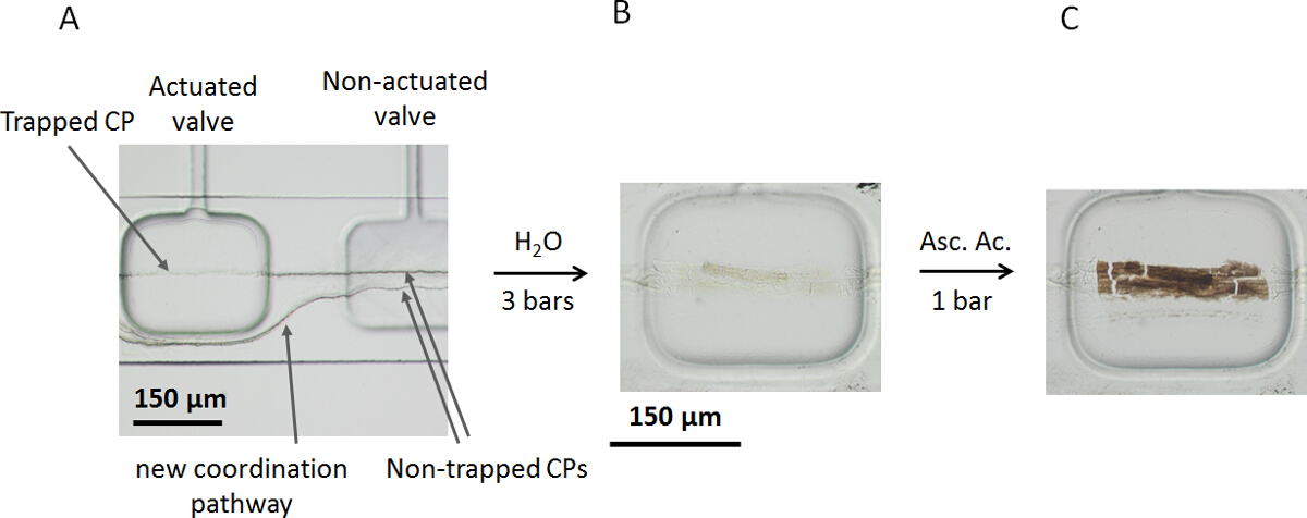
図3Aは、 その場で actuatを介して二層マイクロ流体デバイス内部でのCPを生成するトラップを示しています空気圧ケージのイオン。新しいコーディネート経路は、第一の弁の作動後に生成されていることに注意してください。弁の作動は、二つの試薬 の流れの界面で発生したAg(I)のCys CPの捕捉を確実にし、新たな調整経路( 図3A)の形成を促進します。 2試薬の流れの界面に発生する銀(I)のCys CPの詳細な化学的特徴付けは、以前の研究17,18で見つけることができます。余剰の除去は純水( 図3B)の流量で溶液を試薬後加え、そして、エタノール中の飽和アスコルビン酸溶液は、オンチップの捕捉された構造( 図3C)の制御された化学的還元のためのマイクロ流体チャネルに加えることができます。 1バールの3つのバーからバルブの圧力を減らすことは、クランプエリア18の下に閉じ込められたAg(I)のCys CPの制御された化学処理を優先する。暗褐色に閉じ込められたAg(I)のCysのCPの色の変化があります以前の観察18,29と一致して、金属の一価銀の削減にttributed。

図3.銀のトラッピング(I)のCysのCPおよび制御された化学還元。新しいコーディネート経路のin situ合成したAg(I)のCys CPと世代の捕獲を示す(A)光学顕微鏡画像。 (B)の水の流れに余剰試薬溶液を除去した後のクランプエリアの下に閉じ込められたのCPの顕微鏡写真、およびに(C)、還元反応処理後の同じマイクロバルブの顕微鏡写真。 の拡大版をご覧になるにはこちらをクリックしてください。この図。
ディスカッション
The reported approach can be easily modified to fabricate different valve shapes to afford other applications such as fluid confinement. Indeed, the flexibility of this protocol also allows for modification of the thickness of the bottom layer, and thereby of the PDMS membrane, from a couple of tens to a few hundreds of microns to fulfill any application of interest. Moreover, dimensions of structures in each layer of the device can be optimized for the desired application and various heights of structures on the master molds can be simply achieved by spinning the photoresist at different velocities. Spinning the photoresist at a higher speed results in thinner structures.
To better implement the protocol, a clean room environment for the fabrication of the master molds is substantially essential; otherwise, the fabrication procedure will lead to defective master molds and thereby to unusable microfluidic devices. Two critical aspects should be emphasized in this protocol: i) the constant temperature of the oven that needs to be adjusted to 80 °C and ii) the programmed time period between processes that has to be complied accurately. Any modification of temperature and time frame in the protocol might lead to non-bonded chips, and thus, to non-functional devices.
The "turbulent free" conditions typically encountered in microfluidic systems have recently been employed for the generation of microstructures or molecular materials inside30 and outside single layer microfluidic chips31. In double-layer microfluidic chips, the laminar flow regime, and hence, the interface generated between continuous co-flows can be manipulated using pneumatic cages18,28. These devices also provide for effective control over the synthetic pathway, which in turn leads to precise localization and trapping on surfaces18.
As mentioned earlier, pneumatic actuation in double-layer microfluidic chips has been previously employed for various applications such as cell trapping20, enzymatic activity studies21 and protein crystallization24. However, the main objective of the reported approach is to propose a platform to be used for trapping and directing the coordination pathway of a crystalline molecular material and controlling chemical reactions onto on-chip trapped structures18,25.
The described method does not only allow trapping of anisotropic structures but can be used to localize particles onto surfaces. Future studies can be effectively directed towards the design of new valve shapes for additional application in biology, materials science and sensor technologies. The combination of different valve shapes as well as altered channel heights and membrane thicknesses can be employed to fulfill specific applications, such as chemical studies based on diffusional mixing and the localization of material growth.
A further application of the described microfluidic platforms is in the controlled chemical doping of crystals, which can lead to a rationalized formation of interfaces in crystalline structures19. This approach also provides for a wide range of post-treatments of on-chip trapped structures; a methodology that will undoubtedly open new horizons in materials engineering.
It is important to underline that the number of technologies enabling controlled chemical reactions under dynamic conditions and onto crystalline matter are very limited at present, hence making this approach very attractive in materials-related fields. However, a major limitation of this technology is the use of PDMS. PDMS elastomer is incompatible with many organic solvents, which limits the number of reactions that can be conducted inside these microfluidic chips. In future, the development of other elastomers that can tolerate and be stable against a broader number of organic solvents will be highly required in order to expand this field of research to other materials and chemistries.
開示事項
The authors have nothing to disclose.
謝辞
Authors would like to thank the financial support from Swiss National Science Foundation (SNF) through the project no. 200021_160174.
資料
| Name | Company | Catalog Number | Comments |
| High resolution film masks | Microlitho, UK | - | Features down to 5um |
| SU8 photoresist | MicroChem Corp., USA | SU8-3050 | - |
| Silicon wafers | Silicon Materials Inc., Germany | 4" Silicon Wafers | Front surface: polished, Back surface: etched |
| Silicone Elastomer KIT (PDMS) | Dow Corning, USA | Sylgard® 184 | - |
| Spinner | Suiss MicroTech, Germany | Delta 80 spinner | - |
| UV-Optometer | Gigahertz-Optik Inc., USA | X1-1 | - |
| Mask Aligner | Suiss MicroTech, Germany | Karl Suss MA/BA6 | - |
| SU8 developer | Micro resist technology GmbH, Germany | mr-Dev 600 | - |
| Trimethylsilyl chloride | Sigma-Aldrich, Switzerland | 386529 | ≥97%, CAUTION: Handle it only under fume hood. |
| Biopsy puncher | Miltex GmBH, Germany | 33-31AA-P/25 | 1 mm |
| Biopsy puncher | Miltex GmBH, Germany | 33-31A-P/25 | 1.5 mm |
| Glass coverslip | Menzel-Glaser, Germany | BB024040SC | 24 mm × 60 mm, #5 |
| Laboratory Corona Treater | Electro-Technic Products, USA | BD-20ACV | - |
| PTFE tubing | PKM SA, Switzerland | AWG-TFS-XXX | AWG 20TFS, roll of 100 m |
| Silicone rubber tubing | Hi-Tek Products, UK | - | 1 mm I.D. |
| neMESYS Syringe Pumps | Cetoni GmbH, Germany | Low Pressure (290N) | - |
| High resolution camera | Zeiss, Germany | Axiocam MRc 5 | - |
| Fluorescent inverted microscope | Zeiss, Germany | Axio Observer A1 | Operable at two wavelengths i.e. 350 nm and 488 nm |
| Green polystyrene fluorescent particles | Fisher Scientific, Switzerland | 11523363 | Size: 5.0 um, solid content: 1% |
| Silver nitrate (AgNO3) | Sigma-Aldrich, Switzerland | 209139 | ≥99.0%, |
| L-Cysteine (Cys) | Sigma-Aldrich, Switzerland | W326305 | ≥97.0%, |
| Disposable weighing dish | Sigma-Aldrich, Switzerland | Z154881 | L × W × H : 86 mm × 86 mm × 25 mm |
| Disposable weighing dish | Sigma-Aldrich, Switzerland | Z708593 | Hexagonal, Size XL |
| Plastic spatula | Semadeni, Switzerland | 3340 | L × W : 135 mm x 14 mm |
| Dye, Bemacron ROT E-G | Bezema, Switzerland | BZ 911.231 | Red |
| Stereomicroscope | Wild Heerbrugg, Switzerland | Wild M8 | 500x magnification |
| Disposable scalpels | B. Braun, Switzerland | 233-5320 | Nr. 20 |
| L-Ascorbic acid | Sigma-Aldrich, Switzerland | A4403 | - |
参考文献
- . . Nicolet iS5 User Guide. , (2015).
転載および許可
このJoVE論文のテキスト又は図を再利用するための許可を申請します
許可を申請さらに記事を探す
This article has been published
Video Coming Soon
Copyright © 2023 MyJoVE Corporation. All rights reserved