Method Article
Quantitative Atomic-Site Analysis of Functional Dopants/Point Defects in Crystalline Materials by Electron-Channeling-Enhanced Microanalysis
In This Article
Summary
We provide a general outline of quantitative microanalysis methods for estimating the site occupancies of impurities and their chemical states by taking advantage of electron-channeling phenomena under incident electron beam-rocking conditions, which reliably extract information from minority species, light elements, oxygen vacancies, and other point/line/planar defects.
Abstract
A novel elemental and chemical analysis scheme based on electron-channeling phenomena in crystalline materials is introduced, where the incident high-energy electron beam is rocked with the submicrometric pivot point fixed on a specimen. This method enables us to quantitatively derive the site occupancies and site-dependent chemical information of impurities or intentionally doped functional elements in a specimen, using energy-dispersive X-ray spectroscopy and electron energy-loss spectroscopy attached to a scanning transmission electron microscope, which is of significant interest to current materials science, particularly related to nanotechnologies. This scheme is applicable to any combination of elements even when the conventional Rietveld analysis by X-ray or neutron diffraction occasionally fails to provide the desired results because of limited sample sizes and close scattering factors of neighboring elements in the periodic table. In this methodological article, we demonstrate the basic experimental procedure and analysis method of the present beam-rocking microanalysis.
Introduction
With the demand of downsizing most current industrial products, it is getting more and more important to understand the physical/chemical properties of materials from the microscopic perspective, sometimes in terms of atomic-scale spatial/electronic structures. Novel properties are often discovered unexpectedly when synthesizing materials by trial and error, selecting different numbers or kinds of elements, although current measurement techniques and ab initio theoretical calculations based on density functional theory have enabled design of novel materials with improved properties without time-consuming trial and error experiments. For example, some of the host atoms are substituted with other elements that can possibly improve the target property as results of either experimental or theoretical considerations. In this context, an important component of experimental information is brought about from detailed knowledge of the position of each constituent in the atomic structure of the material.
X-ray and/or neutron diffraction methods are conventionally and widely used not only because the structural analysis based on Rietveld analysis1,2 techniques has been well established and open to the public, but also owing to the development of high-flux X-ray sources (e.g., synchrotron radiation facilities) and modern neutron sources, which are easily accessible to general researchers. However, these techniques require samples with homogeneous structures, and they also require the Rietveld fit between the experimental and theoretical sets of diffracted peak intensities using structural factors. It can thus be difficult to distinguish between different elements if their structural factors are close to each other, such as in X-ray diffraction of neighboring elements in the periodic table.
In most current advanced materials, the compositions, precipitates, grain size, and impurities are adjusted and optimized to maximize the desired role at the nanometer scale. This means that these materials require characterization at the nanometer scale or even sub-nanometer scale to investigate whether they are synthesized as designed. In this context, it could be best achieved using transmission electron microscopy (TEM) and related analytical techniques.
The recent dramatic development of scanning TEM (STEM) in these decades, particularly based on aberration correction technologies, has accelerated a state-of-the-art technique to reveal the structure of a material and its elemental distribution at an atomic scale3,4. This method, however, requires precisely setting the crystalline material parallel to a low-order zone axis and to the extreme stability of the instrument during the measurement, which is a drawback. Hence, we demonstrate an alternative method that requires no such limitations, aberration correction, or even field emission electron gun.
Electron channeling in a crystalline material occurs if an incident electron beam propagates along particular atomic planes or columns, which depends on the direction of the incident high-energy electron beam with respect to the crystal axes, where an appropriate set of Bragg reflections and the excitation error of each reflection in a TEM are selected. The site-specific energy-dispersive X-ray (EDX or sometimes conventionally EDS) analysis technique that uses electron channeling is called the atom location by channeled electron microanalysis (ALCHEMI) method to evaluate the occupancies of host atomic sites by impurities5,6. This method has been extended to a more complex and quantitatively reliable approach, called high-angular-resolution electron-channeling X-ray spectroscopy (HARECXS), to determine impurity/dopant occupancies. This is realized by comparing the experimental beam-rocking curves with theoretical simulations7. This technique is further extended to high-angular-resolution electron-channeling electron spectroscopy (HARECES), which records electron energy loss spectra (EELS) instead of EDX8. This provides information on the site-specific local chemical states of a given element in different atomic environments9,10,11. In cases where each host element occupies a single crystallographic site, a simple linear regression and application of several formulae to the experimental dataset quantitatively determines the site occupancies of doped impurities without any theoretical simulations.
In the following sections, we provide detailed procedures of the method specific to the Jeol JEM2100 STEM system because it is explicitly equipped with the beam-rocking mode in the STEM operation menu. For users of other microscopes, please refer to the descriptions in the final paragraph of the Discussion section of this article.
Protocol
1. Sample preprocess
- Thin film preparation for TEM
- Prepare a sample for the present analysis method using standard transmission electron microscopy (TEM) sample preparation techniques, such as electropolishing for metal materials, ion milling for semiconductors or ceramics, typically less than 100-200 nm for HARECXS, uniformly flat over the area of ~1 μm. Prepare thinner (50-100 nm) samples for HARECES in general.
- Sample mounting to TEM
- Mount the thin film prepared on a double-tilting TEM sample holder, followed by inserting the holder into a TEM equipped with a scanning mode and an EDX detector (Figure 1).
2. TEM operation (specific to JEM2100 STEM with beam-rocking option attached)
- TEM alignment for beam-rocking
- Start the TEM operation. After the routine TEM beam alignment procedure, go to STEM mode by checking Attachment Scanning Image Display (ASID) in the ASID window in the TEM control monitor (TCM, Figure 1 & Figure 2).
- Optical axis alignment
- Click the Rocking button in the ASID window of the TCM and then click the Spot button in the Simple Image Viewer (SIV) to stop beam-rocking (Figure 2). Remove the sample from the field of view. Set the beam-rocking range smaller than ±2° by clicking the Mag increment/decrement buttons.
- Turn the Brightness knob on left operation panel (LOP: Figure 3) clockwise to the limit, followed by turning the OBJ FOCUS COARSE knob of Right Operation Panel (ROP: Figure 3) counterclockwise to an underfocused condition: a caustic spot (Figure 4) appears on the fluorescent viewing screen.
- Press the BRIGHT TILT function key (LOP) and move the caustic spot to the center of the fluorescent screen using a pair of DEF/STIG X/Y knobs (L/ROP).
- Press the Standard Focus button (ROP), and then turn the BRIGHTNESS knob back counterclockwise so that an alternative caustic spot appears on the fluorescent screen.
- Press the F3 function key (ROP) (or click the Spot button in 'Alignment Panel for Maintenance' window on TCM) and move the beam spot to the center using a pair of DEF/STIG X/Y knobs.
- Repeat steps 2.2.2-2.2.5 until the beam position stays at center even if the lens condition is switched at step 2.2.2 and 2.2.4.
- Incident beam collimation and setting its pivot point
- Introduce the third largest condenser aperture at the center of the optical axis by turning the aperture knob clockwise with its position manually adjusted with two attached screws (Figure 1). Then, adjust the condenser lens stigmator to correct the beam shape to be coaxially defocused by turning the BRIGHTNESS knob both ways, using a pair of DEF/STIG knobs with COND STIG key on.
- Press the HT WOBB key (ROP) and adjust the BRIGHT TILT knob to minimize the beam size fluctuation with the change in acceleration voltage. This process adjusts the beam convergence angle minimum. Press the HT WOBB key again to stop HT wobbler.
- Activate maintenance mode (consult the manufacturer's manual). Select JEOL from the menu bar → Scan/Focus window → Scan Control tab in TCM. Then, click the Cor button and click the Scan button instead of Spot in the Image control panel of SIV.
- To minimize the beam shift with beam-rocking, adjust a pair of DEF/STIG knobs, followed by turning the OBJ FOCUS FINE knob slightly counterclockwise. Finally, match the sample and pivot point height using Z control keys (ROP) so that the sample is focused on the fluorescent screen.
- Final beam alignment to obtain electron-channeling pattern of sample
- Move the sample area of interest back to the center, and start beam-rocking by clicking the Scan button in the SIV window. Manually turn clockwise the annular dark field (ADF) detector cylinder (Figure 1) and insert the detector.
- Set the ADF detector position at the center of the beam position by adjusting a pair of DEF/STIG knobs with PLA key on (LOP: Figure 3). Check the STEI-DF button in the Image Select menu of the ASID window and the STEM monitor in the SIV window displays an electron-channeling pattern (ECP). Adjust the Brightness/Contrast in the ASID window to best see ECP. Slightly turn the BRIGHTNESS knob to see the ECP contrast sharpest.
- Data acquisition for HARECXS by EDX
- By operating the STEM in beam-rocking mode, collect the EDX spectra by following the conventional spectral image method (using the spectral imaging function in Figure 5) as a function of beam tilting angles in the x and y directions and display elemental intensity distribution for specified elements, as shown in Figure 5.
NOTE: The intensity distribution pattern is called an ionization channeling pattern (ICP). - Use the Line Scan function in Figure 5 for the 1D tilting measurement of a systematic row of reflections. Yellow arrow appears in the ECP preview to specify the measuring range, as shown in the upper left panel in Figure 5. Stop measurements when sufficient data statistics are obtained for ICPs.
- By operating the STEM in beam-rocking mode, collect the EDX spectra by following the conventional spectral image method (using the spectral imaging function in Figure 5) as a function of beam tilting angles in the x and y directions and display elemental intensity distribution for specified elements, as shown in Figure 5.
3. Data analysis for quantification
- Express X-ray intensity Ix for impurity x in the following form as a function of X-ray intensity Ii of host element i,12

where

NOTE: Here, fix is the fractional occupancy of impurity x on the type i host site, cx is the concentration of impurity x, and ni is the fractional concentration of the type i host element among the total host sites prior to the accommodation of impurity atoms of type x. ki is the k-factor of the type i host element. The additional constant offset βx has been introduced as an extra fitted parameter to account for differences in interaction delocalization and errors in background subtractions. αix can be derived from Eq. (1) by multivariate linear regression for many sampling points of the ICP X-ray intensities. - Derive cx and fix utilizing the condition Σifix = 1 as12

The uncertainties in cx and fix for multiple impurities are readily derived from the error propagation principle:

and

where δ αix is the statistical error obtained in the linear regression from Eq. (1).
Results
The experimental ECP for BaTiO3 and ICPs of Ba-L, Ti-Kα, and O-Kα near the [100] and [110] zone axes are shown in Figure 6A and Figure 6B, respectively. Each constituent element exhibits a specific ICP, indicating that the ICP is atomic site-specific12.
As a fundamental application example, we examined Eu3+-doped Ca2SnO4, which exhibits strong red emission derived from the 5D0-7F2 electric dipole transition of trivalent Eu ions (Eu3+). Considering the ionic radii similarity criterion, it would be more relevant to assume that Eu3+ occupies the Ca2+ sites because Eu3+ is significantly close in size to Ca2+ than to Sn4+. However, Rietveld analysis of powder X-ray diffraction data revealed that Eu3+ equally occupied the Ca2+ and Sn4+ sites, presumably because the local charge neutrality criterion dominates in this case. An Eu and Y co-doped sample Ca1.8Y0.2Eu0.2Sn0.8O4 was then synthesized because Y3+ ions with a smaller ionic radius preferentially occupy smaller cation (Sn4+) sites, expelling larger Eu3+ ions out of the Sn4+ site into the larger Ca2+ site without changing the charge balance. As expected, Ca1.8Y0.2Eu0.2Sn0.8O4 exhibited a stronger emission than the Ca1.9Eu0.2Sn0.9O4 sample. The stronger red emission in the co-doped sample is explained by the increased fraction of Eu3+ ions occupying the asymmetric Ca site, coordinated by seven oxygen atoms, which enhances the electric dipole moment compared to that of the symmetric six-coordinated Sn site.
A series of Eu and Y co-doped polycrystalline samples with nominal compositions of Ca1.9Eu0.2Sn0.9O4 and Ca1.8Eu0.2Y0.2Sn0.8O4 were prepared, and the site occupancies of the dopants were determined by the present method.
Figure 7 shows the ECP and ICPs of Ca-K, Sn-L, O-K, Eu-L, and Y-L for the Ca1.8Eu0.2Y0.2Sn0.8O4 sample near the [100] zone. The Eu-L ICP was closer to the Ca-K ICP, whereas the Y-L ICP was closer to Sn-L ICP. This suggests that the Eu and Y occupation sites could be biased, as expected. The coefficients, αix for i = Ca, Sn, and x = Eu, Y derived using Eq. (1), where nCa = 2/3 and nSn = 1/3. The k-factors of the constituent elements are calibrated in advance using a reference material with a known composition, the detailed discussion of which is found in ref.12. The site occupancies fix (Eq. (3)) of the impurities, and the impurity concentrations c of all the samples are tabulated in Table 1.
In Ca1.9Eu0.2Sn0.9O4, Eu3+ occupied the Ca2+ and Sn4+ sites equally, consistent with the results of the XRD-Rietveld analysis. In contrast, Eu3+ and Y3+ occupied the Ca2+ and Sn4+ sites at ratios of approximately 7:3 and 4:6, respectively, in the co-doped samples, significantly biased as expected, but also maintaining the charge neutrality condition within the present experimental accuracies12.
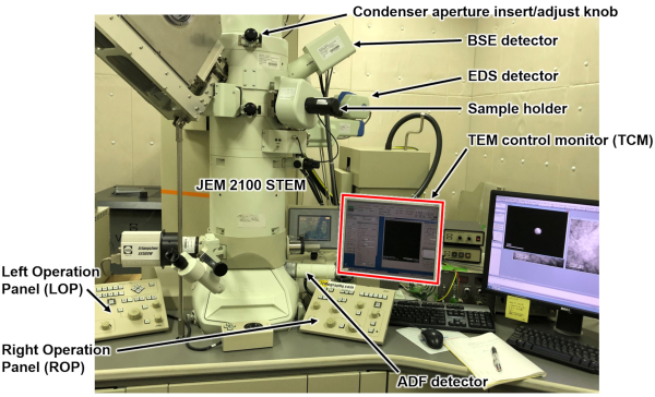
Figure 1: Instrumental outlook. Jeol JEM2100 STEM and its associated monitors, detectors, and operation panel configurations. Please click here to view a larger version of this figure.
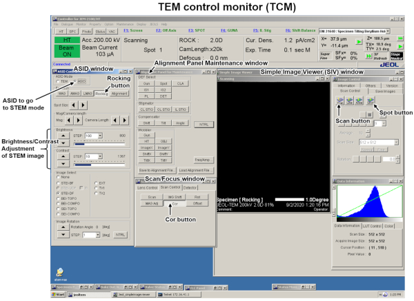
Figure 2: Layout of TEM control monitor (TCM). Control windows necessary for the present method are displayed and key functions and buttons are labeled. Please click here to view a larger version of this figure.
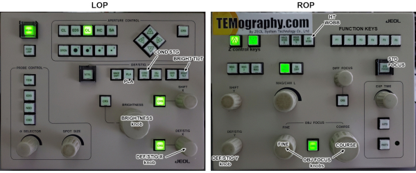
Figure 3: Left/right operation panels of the S/TEM. (Left) Left operation panel (LOP). (Right) Right operation panel. The function keys and operation knobs necessary for the present method are labeled. Please click here to view a larger version of this figure.
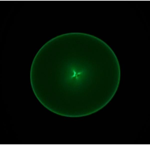
Figure 4: Caustic spot image on the fluorescent screen. The diameter of the spot ranges a few centimeters on the screen, depending on the defocus value. Please click here to view a larger version of this figure.
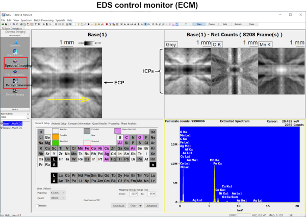
Figure 5: Appearance of EDS control monitor. Electron-channeling pattern (ECP) preview in upper left panel specifies the area of measurement. For 1D tilting measurements, X-ray Linescan is selected in the leftmost panel and the range of measurement is indicated by the yellow arrow in the ECP preview. Periodic table in the lower left panel selects the elements of the ionization channeling patterns (ICPs) to be displayed in upper right panel. Lower right panel displays the accumulated EDS pattern in real-time. Please click here to view a larger version of this figure.
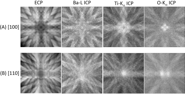
Figure 6: Experimental ECPs and ICPs. (A: from left to right) ECP and ICPs of Ba-L, T-Ka, and O-Ka emissions from BaTiO3 obtained by beam-rocking near [100] zone axis. (B: from left to right) Same as (A) near [110] zone axes. This figure has been modified from [12]. Please click here to view a larger version of this figure.
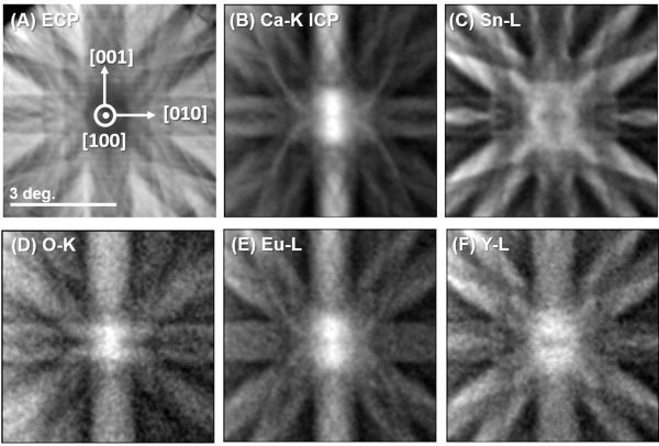
Figure 7. ECP and corresponding X-ray ICPs from Ca1.8Eu0.2Y0.2Sn0.8O4 by beam-rocking near the [100] zone axis. (A) ECP. (B-F) ICPs of Ca-Ka, Sn-L, O-Ka, O-Ka, Eu-L, and Y-L emissions, respectively. This figure has been modified from [12]. Please click here to view a larger version of this figure.
| Sample | Dopant | αCa | αSn | fCa | fSn | c x (x = Eu or Y) |
| Ca1.9Eu0.2Sn0.9O4 | Eu | 1.71±0.001 | 0.083±0.001 | 0.57±0.001 | 0.43±0.002 | 0.061±0.001 |
| Ca1.8Eu0.2Y0.2Sn0.8O4 | Eu | 0.162±0.001 | 0.077±0.001 | 0.78±0.003 | 0.22±0.008 | 0.088±0.006 |
| Y | 0.040±0.002 | 0.265±0.009 | 0.28±0.002 | 0.72±0.001 | 0.118±0.004 |
Table 1. Derived parameters (defined in text) of the samples of Ca2-xEuxSn1-yYyO4 where (x, y) = (0.2, 0.0) and (0.2, 0.2).
Discussion
Critical steps in the protocol are the ability to accurately align the incident rocking beam that has a small convergence angle with the pivot point, which is immobile at the specified area described in steps 2.2-2.3. A collimated incident beam with a convergence semi-angle of approximately no larger than 2 mrad was used. A beam size of 400 nm and diameter of 1 µm can be selected by setting the condenser aperture #4 (10 μm in diameter) and #3 (30 μm) in the present hardware system.
The advantages of the present method are that (i) no advanced STEM instruments such as aberration-corrected STEM or even field emission electron gun is necessary; (ii) many sampling points (e.g., ~4,000 points for a scan area of 64 × 64 pixels2) can be automatically collected with high efficiency, while operating the conventional STEM spectral imaging procedure on the analyzer side, and (iii) multiple spectroscopic methods such as EDX, EELS, and cathodoluminescence can be concurrently operated in a single integrated system, which enables multimodal analysis13.
Since the experimental ICPs can be precisely predicted by theoretical simulation, the method can be applied not only to cases where the crystal of interest contains multiple inequivalent atomic sites for a doped element14. Further extensions are ongoing, such as to detect the vacancy concentrations and associated displacements of host elements15, and even the ordering of dopants segregated along the grain boundaries of ceramics. The present method can provide a significant alternative technique applicable to relatively thick samples in contrast to atomic column-by-column analysis using aberration-corrected STEM, which requires the preparation of very thin high-quality samples (< 10 nm).
Atom site-selective electronic state analysis using TEM-EELS (HARECES) rather than EDX is feasible8,9,10,11. For automatic measurement it is recommended to use 'ALCHEMI option' in a beam controlling software 'QED,' running on the Gatan Microscope Suite, supplied by HREM Research Inc16. In HARECES measurement, it is necessary to ensure that the transmitted beam is away from the EELS detector position and perpendicular to the systematic row in the beam tilting sequence8.
A limitation of this method is the minimum beam size of the incident electron beam, which limits the minimum measured area to approximately 400 nm. This is due to the aberration of the TEM lens system wherein the pivot center moves farther than the beam radius for a smaller beam size, which could be amended in the future by modifying the TEM deflector lens current setting to compensate for the beam wandering.
If the microscope used does not have beam-rocking mode, a very similar operation is achieved using QED software, which also addresses the limitation, as the software can rectify the pivot point moving even in the nano-beam mode. For S/TEMs manufactured by FEI Company (now part of Thermo Fisher Scientific), TIA scripting, open-source code can manage all S/TEM functions and attached detectors via a PC. Sequential EDX/EELS data acquisitions with successive incident beam tilting were performed using the scripting program TIA running on the TEM imaging and analysis platform13.
Disclosures
The authors have nothing to disclose.
Acknowledgements
This work was partly supported by Grants-in-Aid for Scientific Research on Kiban-kenkyu A (No. 26249096), Innovative Areas "Nano Informatics" (No. 25106004), and Wakate-kenkyu B (No. 26870271) from the Japan Society of the Promotion of Science.
Materials
| Name | Company | Catalog Number | Comments |
| Electron Energy-Loss Spectrometer | Gatan Inc. | Enfina1000 | Parallel EELS detector |
| Energy dispersive X-ray detector | JEOL Ltd. | SD30GV | EDS silicon drift detector |
| Gatan Microscope Suite (GMS) | Gatan Inc. | ver. 2.3. | Integrated software platform for controling cameras, detectors, S/TEM and data analysis |
| QED | HREM Research Inc. | for GMS 2.3 32bit | beam controlling software, running on the Gatan Microscope Suite |
| scanning transmission electron microscope | JEOL Ltd. | JEM-2100 | Beam-rocking mode option in ASID controlling window |
| TEMCON | JEOL Ltd. | Control software for JEM 2100 | |
| Thermo NSS software | Thermo Fischer Scientific Inc., USA | EDS control software |
References
- Rietveld, H. M. A profile refinement method for nuclear and magnetic structures. Journal of Applied Crystallography. 2, 65-71 (1969).
- Izumi, F., Ikeda, T. A Rietveld-analysis program RIETAN-98 and its applications to zeolites. Materials Science Forum. 321-324, 198-203 (2000).
- Rose, H. H. Optics of high-performance electron microscopes. Science and Technology of Advanced Materials. 9, 014107 (2008).
- Muller, D. A., et al. Atomic-scale chemical imaging of composition and bonding by aberration- corrected microscopy. Science. 319, 1073-1076 (2008).
- Spence, J. C. H., Taftø, J. ALCHEMI: A new technique for locating atoms in small crystals. Journal of Microscopy. 130, 147-154 (1982).
- Taftø, J., Spence, J. C. H. Crystal site location of iron and trace elements in an Mg-Fe olivine using a new crystallographic technique. Science. 218, 49-51 (1982).
- Yasuda, K., Yamamoto, T., Matsumura, S. The atomic structure of disordered ion tracks in magnesium aluminate spinel. Journal of Microscopy. 59, 27 (2007).
- Tatsumi, K., Muto, S. Local electronic structure analysis by site-selective ELNES using electron channeling and first-principles calculations. Journal of Physics Condensed Matter. 21, 1-14 (2009).
- Yamamoto, Y., Tatsumi, K., Muto, S. Site-selective electronic structure of aluminum in oxide ceramics obtained by TEM-EELS analysis using the electron standing-wave method. Materials Transactions. 48, 2590-2594 (2007).
- Tatsumi, K., Muto, S., Nishida, I., Rusz, J. Site-specific electronic configurations of Fe 3d states by energy loss by channeled electrons. Applied Physics Letters. 96, 201911 (2010).
- Tatsumi, K., Muto, S., Rusz, J. Energy loss by channeled electrons: A quantitative study on transition metal oxides. Microscopy and Microanalysis. 19, 1586-1594 (2013).
- Muto, S., Ohtsuka, M. High-precision quantitative atomic-site-analysis of functional dopants in crystalline materials by electron-channelling-enhanced microanalysis. Progress in Crystal Growth and Characterization of Materials. 63, 40-61 (2017).
- Yamamoto, Y., et al. Quantitative analysis of cation mixing and local valence states in LiNixMn2-xO4 using concurrent HARECXS and HARECES measurements. Microscopy. 65, 253-262 (2016).
- Ohtsuka, M., Muto, S., Tatsumi, K., Kobayashi, Y., Kawata, T. Quantitative determination of occupation sites of trace Co substituted for multiple statistical beam-rocking TEM-EDXS analysis. Microscopy. 65, 127-137 (2016).
- Ohtsuka, M., Oda, K., Tanaka, M., Kitaoka, S., Muto, S. 2D-HARECXS analysis of dopant and oxygen vacancy sites in Al-doped yttrium titanate. J. Amer. Ceram. Soc. , (2021).
- . QED for DigitalMicrograph Available from: https://www.hremresearch.com/Eng/plugin/QEDEng.html (2020)
Reprints and Permissions
Request permission to reuse the text or figures of this JoVE article
Request PermissionExplore More Articles
This article has been published
Video Coming Soon
Copyright © 2025 MyJoVE Corporation. All rights reserved