
Method Article
Fabrication of Schottky Diodes on Zn-polar BeMgZnO/ZnO Heterostructure Grown by Plasma-assisted Molecular Beam Epitaxy
In This Article
Summary
Attainment of high-quality Schottky contacts is imperative for achieving efficient gate modulation in heterostructure field effect transistors (HFETs). We present the fabrication methodology and characteristics of Schottky diodes on Zn-polar BeMgZnO/ZnO heterostructures with high-density two dimensional electron gas (2DEG), grown by plasma-assisted molecular beam epitaxy on GaN templates.
Abstract
Heterostructure field effect transistors (HFETs) utilizing a two dimensional electron gas (2DEG) channel have a great potential for high speed device applications. Zinc oxide (ZnO), a semiconductor with a wide bandgap (3.4 eV) and high electron saturation velocity has gained a great deal of attention as an attractive material for high speed devices. Efficient gate modulation, however, requires high-quality Schottky contacts on the barrier layer. In this article, we present our Schottky diode fabrication procedure on Zn-polar BeMgZnO/ZnO heterostructure with high density 2DEG which is achieved through strain modulation and incorporation of a few percent Be into the MgZnO-based barrier during growth by molecular beam epitaxy (MBE). To achieve high crystalline quality, nearly lattice-matched high-resistivity GaN templates grown by metal-organic chemical vapor deposition (MOCVD) are used as the substrate for the subsequent MBE growth of the oxide layers. To obtain the requisite Zn-polarity, careful surface treatment of GaN templates and control over the VI/II ratio during the growth of low temperature ZnO nucleation layer are utilized. Ti/Au electrodes serve as Ohmic contacts, and Ag electrodes deposited on the O2 plasma pretreated BeMgZnO surface are used for Schottky contacts.
Introduction
Heterostructure field effect transistors (HFETs) based on two dimensional electron gas (2DEG) have a promising potential for the applications in high speed electronic devices1,2,3. Zinc oxide (ZnO) as a wide bandgap (3.4 eV) semiconductor with high electron saturation velocity has gained considerable attention as a platform for HFETs4,5. Conventionally used barrier material MgZnO ternary necessitate a very high Mg content (>40%) grown at low substrate temperatures (300 °C or lower)6,7, and as such these structures are apt to degrade under high power operations and during thermal treatments, even if the unwanted charge density in the barrier is low enough for gate modulation. To circumvent this obstacle, we have proposed and adopted BeMgZnO as the barrier, in which the strain sign in the barrier can be switched from compressive to tensile via the incorporation of beryllium (Be), making the spontaneous and piezoelectricpolarizations to be additive. As a result, high 2DEG concentration can be achieved with relatively moderate Mg content. Utilizing this approach, high 2DEG densities is observed near the plasmon-LO phonon resonance (~7×1012 cm-2) in BeMgZnO/ZnO heterostructures while the Mg content below is 30% and the Be content is only at 2~3%8.
Due to its similar crystal symmetry, UV and visible light transparency, robust physical and chemical properties, and low cost, c-plane sapphire is widely employed for epitaxy of both GaN and ZnO. Thanks to the remarkable progress achieved in the growth technology of GaN-based electronic and optoelectronic devices on saphhire, high quality GaN templates can be easily produced on sapphire substrates by using AlN or low-temperature (LT) GaN buffer, despite its large lattice mismatch of 16% with sapphire9. Epitaxial growth of ZnO, which has an even larger in-plane lattice mismatch of 18% with sapphire, is relatively well understood for O-polar variety, while the growth of Zn-polar material in two-dimensional mode is not well established. Due to the moderate lattice mismatch of 1.8%, epitaxy of ZnO on GaN is an attractive alternative.
Both MOCVD and MBE are the most successful semiconductor deposition techniques for fabricating high-quality thin films and heterostructures with high reproducibility. The main reason that MBE is less popular than MOCVD for epitaxy of GaN is the cost and inadequacy for mass production. The growth rate in GaN by MOCVD can be several micrometers per hour, and tens of 2 inch (50 mm) diameter wafers or those as large as 6-8" can be grown in one run9. Here, we also adopt MOCVD for the growth of GaN in our study. For the growth of ZnO-based heterostructures, however, more reports on the formation of 2DEG are realized by MBE at the present time prior to the commercialization of the potential applications10,11,12. Recently, we have developed MBE growth of high quality ZnO heterostructures with an accurate control of surface polarity on Ga-polar GaN templates13. It was found that with Zn pre-exposure treatment, ZnO layers so grown exhibited Zn-polarity when nucleated with low VI/II ratios (<1.5), while those nucleated with VI/II ratios above 1.5 exhibited O-polarity. To avoid parallel conduction channel through GaN templates, we adopted carbon compensated semi-insulating GaN MOCVD grown under low-pressure conditions on AlN buffer for the subsequent growth of ZnO-based HFET structures.
Prior to our work14, there has been no reports on the investigation of Schottky diodes on BeMgZnO/ZnO heterostructures. Only several studies have reported on Schottky contacts to MgZnO15,16, e.g., with an ideality factor of 2.37, a barrier height of 0.73 eV, and a rectification ratio of only 103 15. Various Schottky metals have been used for ZnO17, and among them, silver (Ag) has been widely adopted, due to a relatively high Schottky barrier height of 1.11 eV on bulk ZnO with an ideality factor of 1.08 18.
In this work, we aim to fabricate high-quality Schottky diodes for the applications in ZnO-based high-speed HFET devices. The following protocol applies specifically to the fabrication of Ag/BeMgZnO/ZnO Schottky diodes by e-beam evaporation of Ag on the BeMgZnO/ZnO heterostructures grown by plasma-assisted MBE on MOCVD-deposited GaN templates.
Protocol
1. Growth and Preparation of GaN Template for MBE Growth
- Growth of semi-insulating GaN template by MOCVD
- Ensure that the gate valve isolating the load-lock chamber from the reactor is closed. Vent the load-lock with N2 to atmospheric pressure. Open the load-lock to take out the substrate holder.
- Load the 2-inch sapphire substrate on the holder and then place the holder back into the load lock. Pump down the load-lock pressure down to 2.5×10⁻² Torr by a mechanical dry pump.
- Vent the load-lock with N2 to equalize its pressure with that in the reactor chamber (15 Torr).
- Open the load-lock isolation gate valve and load the holder into the sample holder assembly in the reactor. Turn on the rotation motor and set the substrate-holder rotation speed of 100 rpm. Then close the gate valve.
- Ensure that the cooling water is running, both H2 and NH3 supply is sufficient, mass flow controller (MFC) and pressure controller (PC) readings are the same as the setpoints, and the substrate holder is rotating.
- Switch the system gas from N2 to H2. Turn on the in situ optical reflectance monitor.
- Initiate the growth by starting the recipe file, which preinstalls all the growth parameters including the ramping of substrate temperatures, gas flow rates, and reactor pressure, and switching of valves.
- Ramp up the reactor pressure to 30 Torr in 3 min and the substrate temperature to 1055 °C to desorb residual contaminations from the substrate surface for 3 min in H2 environment.
- Ramp down the substrate temperature to 941 °C for the nucleation and growth of low-temperature (LT) AlN buffer layer.
- Stabilize the trimethylaluminum (TMAl) flow as 12 standard cubic centimeter per minute (sccm) and ammonia (NH3) flow as 7 sccm and the substrate temperature for 3 min.
- Initiate the growth of the LT-AlN layer by switching TMAl from vent to the run line.
- Control the thickness of the LT-AlN layer by using a custom-built reflectivity measurement system, which includes a 637-nm laser diode, a p-i-n Si photodetector, and a Labview-based software. Determine the growth rate from the period of reflectivity oscillations19,20. In selected samples, use cross-sectional scanning electron microscopy and transmission electron microscopy images to confirm the accuracy of in situ monitoring.
- Keep the growth for 6 min to reach a thickness of ~20 nm, then ramp up the substrate temperature to 1100 °C in 3 min without a growth interruption and continue the growth of AlN layer to a thickness of 300 nm, as monitored by the evolution of the oscillation of the in situ optical reflectance.
- Switch TMAl from run to vent and then to idle line to stop the AlN growth. Stabilize the trimethylgallium (TMGa) flow at 15.5 sccm, ramp up the NH3 flow to 7000 sccm and stabilize for 1 min. Ramp up the reactor pressure to 76 Torr in 1 min. Ramp up the substrate temperature to 1107 °C in 1 min.
- Nucleate and grow a GaN recovery layer with a thickness of ~400 nm, while monitoring the reflectivity evolution. Initially the reflectivity exhibits a sharp decrease when GaN islands nucleate on AlN surface and then recovers the intensity to the original level corresponding to an atomically flat surface when the islands coalesce.
- Ramp up the substrate to 1124 °C in 2 min. Grow the high-temperature semi-insulating GaN layer with a thickness of ~2.5 μm. Stop the growth by switching TMGa from run to vent and then to idle line.
- Cool down the substrate to room temperature over a 40 min period.
- Ramp down the reactor pressure to 15 Torr over a 1.5 min period.
- Unload the substrate from the reactor by following the reverse procedure of steps 1.1.1-1.1.4.
- GaN template preparation and loading to MBE reactor
- Cut the 2-inch GaN template into 6 equal pie-shaped pieces by using a diamond scriber.
- Prepare aqua regia acid solution inside the acid fume hood by adding nitric acid (HNO3, 68.0-70.0 w/w%, 50 mL) to hydrochloric acid (HCl, 36.5-38.0 w/w%, 150 mL) slowly into a quartz beaker.
- Put the aqua regia beaker on a hot plate with a temperature of 220 °C.
- After the appearance of an orange/red color and gas bubbles, soak one pie-shaped GaN template in the solution and boil it for 10 min.
- Rinse the GaN template in running de-ionized (DI) water for 3 min.
- Soak the GaN template in HCl (36.5-38.0 w/w%):H2O solution (1:1) for 3 min to remove Ga oxide.
- Rinse the GaN template in running DI water for 5 min.
- Dry the template with N2 gas.
- Put the cleaned GaN template on a Mo holder and load it into MBE load-lock chamber immediately.
- Start pumping down the load-lock by a mechanical dry pump.
2. MBE Growth of BeMgZnO/ZnO Heterostructures
- Preparation of the effusion cells
- After pumping down the load-lock for 1 h, start the preparation of the Zn, Mg, Be effusion cells. Set the upper zone temperature of the double-zone Zn cell to 525 °C with a ramping rate of 17 °C/min, wait for 5 min then ramp down to 515 °C with a ramping rate of 5 °C/min. Set the Mg cell temperature to 570 °C with a ramping rate of 15 °C/min, after reaching the set point, wait for 10 min then ramp the Mg cell down to 300 °C. Set the Be cell temperature to 900 °C with a ramping rate of 10 °C/min, after reaching the set point, wait for 3 min then ramp the cell down to 650 °C.
- After 30 min, set the lower zone temperature of the double-zone Zn cell to 360 °C with a ramping rate of 10 °C/min.
- After pumping down the load-lock for 2 h to reach a pressure of ~5×10⁻⁷ Torr, turn on the reflection high-energy electron diffraction (RHEED) system, and load the GaN template into the MBE chamber.
- Tune the angle of the GaN template by rotating the manipulator to monitor the RHEED pattern evolution along [1-100] azimuthal direction.
- Set the lower zone temperature of the double-zone Zn cell to 355 °C with a ramping rate of 10 °C/min.
- Polarity control of ZnO on GaN and growth of LT-ZnO buffer
- Ramp up the substrate temperature to 615 °C with a ramping rate of 13.6 °C/min to desorb the residual contaminations from the substrate surface for 15 min.
- Ramp down the substrate temperature from 615 to 280 °C with a ramping rate of 13.6 °C/min for the growth of LT-ZnO. When the temperature reaches 550 °C, open the Zn cell shutter to expose the GaN template surface with Zn flux. Turn on O2 plasma power supply, set the power as 100 W, and check to verify that O2 gas line is closed.
- When the temperature reaches 280 °C, set the O2 plasma power to 400 W, set the O2 flow rate to 0.3 sccm to ignite the plasma then decrease the O2 flow rate to 0.25 sccm.
- Wait for 1 min, then open the O2 shutter to start the growth of LT-ZnO buffer layer.
- Record a RHEED pattern every 5 min. After growing for approximately 15 min corresponding to a buffer thickness of ~20 nm, when the RHEED pattern changes from stripes (2D mode) to elliptical spots (3D mode), close both Zn and O2 shutters to stop the growth.
- Set the O2 flow rate to 0.4 sccm, and set the substrate temperature to 730 °C with a ramping rate of 13.6 °C/min to anneal the LT-ZnO buffer layer. Set the lower zone temperature of the double-zone Zn cell to 345 °C with a ramping rate of 10 °C/min for the growth of HT-ZnO layer.
- When the substrate temperature reaches the set-point of 730 °C, wait for 5 min and check the ZnO surface by RHEED. When the RHEED pattern transits from 3D to 2D, stop annealing by ramping down the substrate temperature to 700 °C.
- Growth of high-temperature ZnO layer
- When the substrate temperature reaches 700 °C and stabilizes, increase the O2 flow rate to 3.2 sccm.
- Start the growth of HT-ZnO layer by opening both Zn and O2 shutters concurrently.
- Grow the HT-ZnO layer for ~140 min to reach a thickness of ~300 nm. Record the RHEED patterns several times during the growth to confirm the 2D growth mode.
- Stop the growth of HT-ZnO layer by closing both Zn and O2 shutters concurrently.
- Growth of BeMgZnO barrier
- Set the O2 flow rate to 0.3 sccm, set the Be cell temperature to 820 °C with a ramping rate of 10 °C/min, set the Mg cell temperature to 510 °C with a ramping rate of 15 °C/min, and set the substrate temperature to 325 °C with a ramping rate of 13.6 °C/min for the growth of the BeMgZnO barrier.
- When the substrate temperature stabilizes, increase the O2 flow rate to 1.25 sccm, and start the growth by concurrent opening the Zn, Mg, Be, and O2 shutters.
- Grow the BeMgZnO barrier layer for ~12 min to reach a thickness of ~30 nm. Record RHEED patterns several times during the growth to monitor the growth mode evolution.
- Stop the growth of BeMgZnO layer by closing the Mg and Be shutter, while keeping the Zn and O2 shutter open for 1 min to have a ~2 nm thick ZnO cap layer.
- Finish the growth by closing both Zn and O2 shutters.
- Ramp down the substrate temperature to its standby temperature 150 °C. Decrease the O2 flow rate to 0.25 sccm.
- When the substrate temperature is below 250 °C, decrease the O2 plasma power to 100 W, turn off O2 plasma power supply, decrease the O2 flow rate to 0, close the O2 gas line, and cool down the cell temperatures to standby conditions.
- Wait for the substrate temperature to reach the standby temperature 150 °C, open the growth chamber gate valve and unload the wafer holder to the load-lock chamber.
- Vent the load-lock chamber with N2 gas and take out the sample.
3. Characterizations
- Roughly measure the thickness of the sample by using a step-profiler, through the covered area on the edge of the sample.
- Evaluate the thickness, strain and structural quality of the heterostructure by using high resolution X-Ray diffraction (HRXRD) (2q-w scans of (0002) reflection).
- Cut the sample into 5×5 mm2 square piece by using a diamond scriber. Investigate the electronic properties of the sample by using temperature dependent Hall Effect measurements in the van der Pauw geometry, with indium (In) dots as contact electrodes.
- Check the surface morphology by using atomic force microscopy (AFM).
4. Fabrication of Schottky Diodes
- Fabrication of Ohmic contacts on BeMgZnO/ZnO heterostructures
- Degrease the sample (~20×20 mm2 in size) with acetone in an ultrasonic cleaner for 5 min, followed by cleaning with methanol in the ultrasonic cleaner for 5 min, rinsing in DI water for 5 min, and blowing dry with N2.
- Spin coat photoresist with 1000 rpm for 3 s and then 3000 rpm for 30 s.
- Soft bake the photoresist at 100 °C for 140 s.
- Expose with UV light through the Ohmic contact mask at 6.5 mW UV lamp power for 2.38 min on photolithography mask aligner.
- Post bake the photoresist at 110 °C for 80 s.
- Develop in a developer for 60 s with a shaking frequency of 1/s.
- Rinse in DI water for 3 min, and blow dry with N2.
- Load the sample into the electron beam evaporator.
- Without heating the sample, deposit Ti/Au with a thickness of 30/50 nm, as measured by quartz crystal thickness monitor.
- Lift-off in acetone, followed by cleaning in methanol for 5 min, rinsing in DI water for 5 min, and blowing dry with N2.
- Anneal the contact by rapid thermal annealer (RTA) at 300 °C for 30 s.
- Check contact resistance through transition line model (TLM) measurement21.
- Fabrication of Schottky contacts on BeMgZnO/ZnO heterostructures
- Follow steps 4.1.1-4.1.7 for photolithography of Schottky contact.
- Treat the sample surface with remote O2 plasma for 5 min with an O2 flow of 35 sccm and an RF power of 50 W.
- Follow steps 4.1.8-4.1.10 for the deposition of Ag with a thickness of 50 nm.
- Characterize the obtained structure by I-V measurements for the Schottky diodes17.
Results
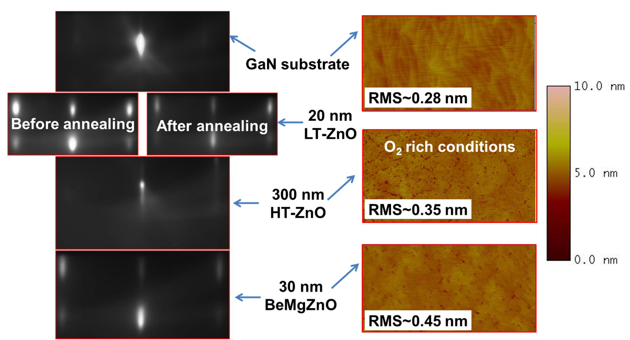
The left column of Figure 1 shows the evolution of RHEED pattern recorded along the [1-100] azimuthal direction during MBE growth of a Be0.02Mg0.26ZnO/ZnO heterostructure with a 300 nm thick HT-ZnO layer and a 30 nm thick Be0.02Mg0.26ZnO barrier. The right column shows representative surface morphologies at different growth stages (not from the same sample). As evidenced from the appearance of a spotty RHEED pattern, the LT-ZnO buffer layer is of three-dimensional (3D) island growth mode nature. Its surface morphology was improved by thermal annealing treatment at a temperature above 700 °C. It is clearly seen that the surface transformed from 3D to 2D morphology. The subsequent HT-ZnO layer continues to grow in a 2D mode, followed by the 2D growth of Be0.02Mg0.26ZnO layer without the formation of a second phase. AFM measurements have shown that the GaN template has a root mean square (RMS) roughness of 0.28 nm for 5×5 μm2 scan. A smooth surface with an RMS roughness of 0.35 nm is obtained for the HT-ZnO layer without a barrier by growing under O-rich condition and an RMS roughness of 0.45 nm is observed after the growth of BeMgZnO barrier.
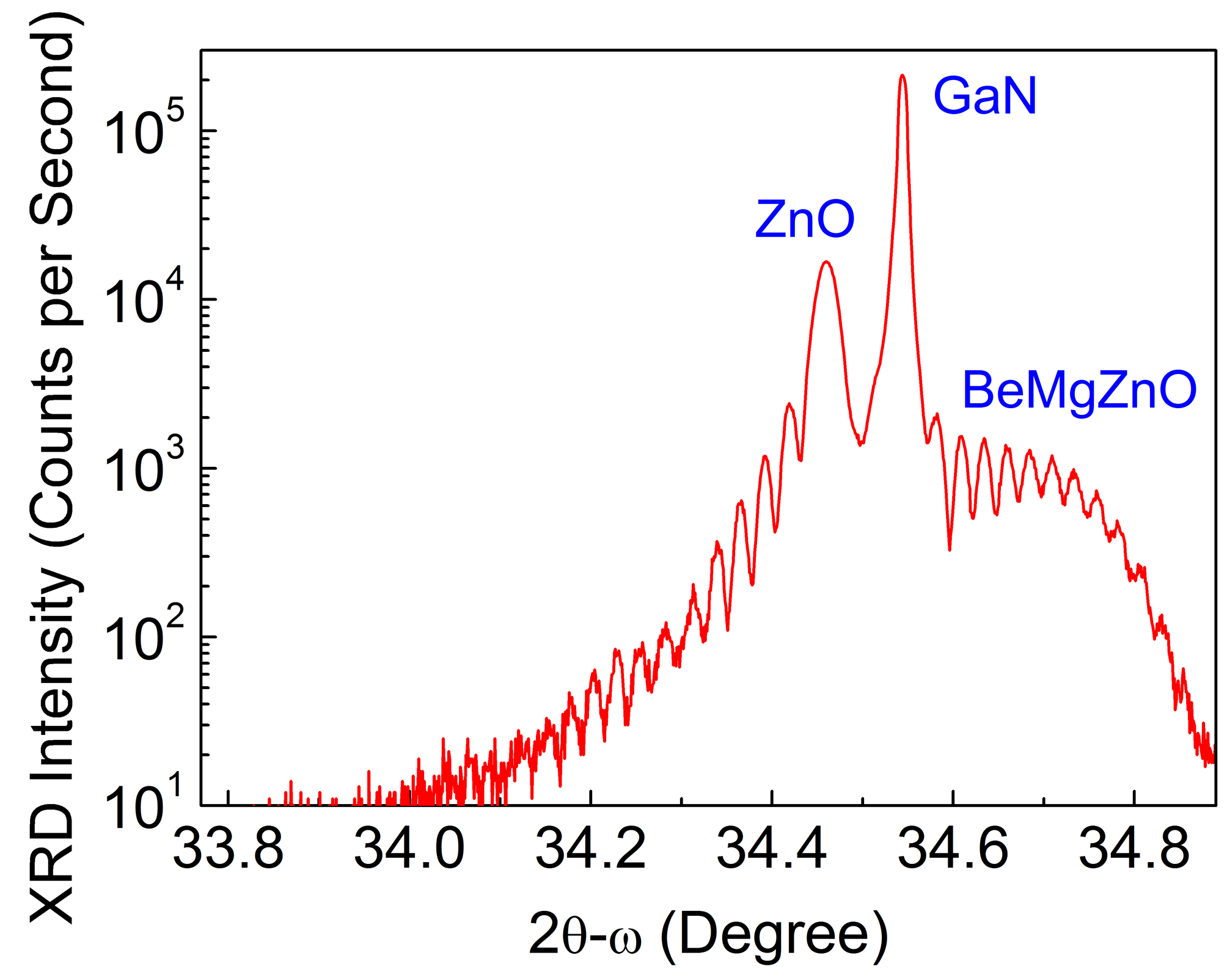
HRXRD triple-axis 2θ-ω scan for a typical Zn-polar Be0.02Mg0.26ZnO/ZnO heterostructure with a 300 nm thick HT-ZnO layer, and a 50 nm thick Be0.02Mg0.26ZnO barrier layer is shown in Figure 2. The reflections at 34.46 o, 34.54 o, and 34.75 o are consistent with (0002) reflections of ZnO, GaN, and Be0.02Mg0.26ZnO, respectively. Note that the broadening of the reflection from Be0.02Mg0.26ZnO is due to its thinness. The tensile biaxial strain in the ZnO layer is an indication of the Zn-polar heterostructure, as investigated in our previous study13. Be and Mg contents in the BeMgZnO quaternary were calculated from the Bragg angle of its XRD (0002) reflection and emission photon energy in LT-photoluminescence (LT-PL) spectrum measured at 13 K (not shown).
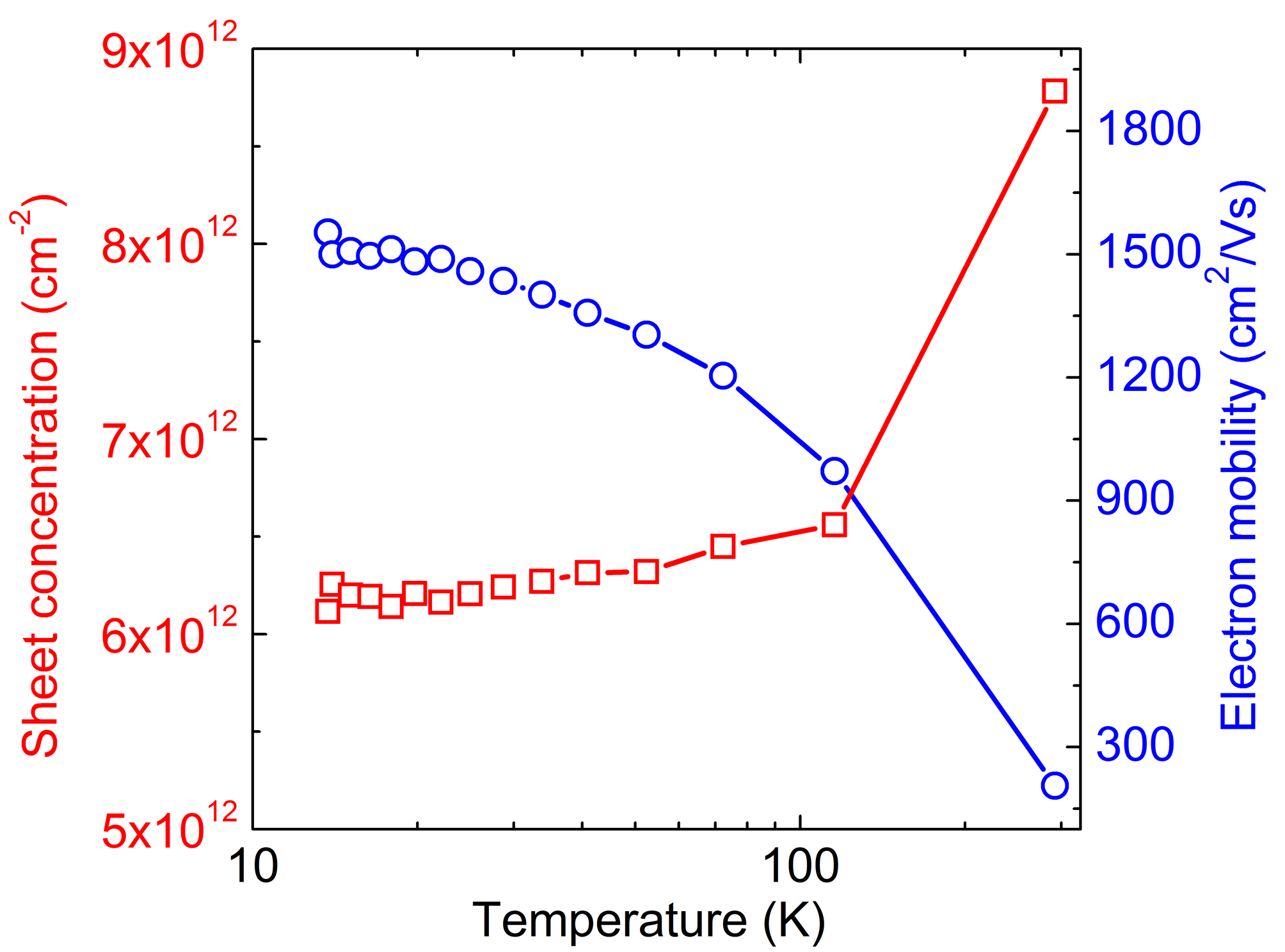
Figure 3 shows the results of temperature-dependent Hall Effect measurements for a Be0.02Mg0.26ZnO/ZnO heterostructure. The sheet carrier concentration reduced from 8.8×1012 cm-2 to 6.4×1012 cm-2 when the sample was cooled down from room temperature (293 K) to approximately 100 K. With further cooling to 13 K, the sheet carrier concentration saturates at 6.2×1012 cm-2. This finding manifests that the observed reduction in electron concentration is originated from the contributions from parallel conduction channels which include defective nucleation layer and HT-ZnO layer as well as the Be0.02Mg0.26ZnO barrier, if any. This trend has also been reported for MgZnO/ZnO heterostructures10,22. The electron mobility in the Be0.02Mg0.26ZnO/ZnO heterostructure monotonically increases with decreasing temperature; both the 293 K mobility of 206 cm2/Vs and the 13 K mobility of 1550 cm2/Vs are comparable to the values in the literature22,23. The evolution of the electronic properties as a function of temperature clearly indicates the presence of 2DEG at the Be0.02Mg0.26ZnO/ZnO heterointerface.
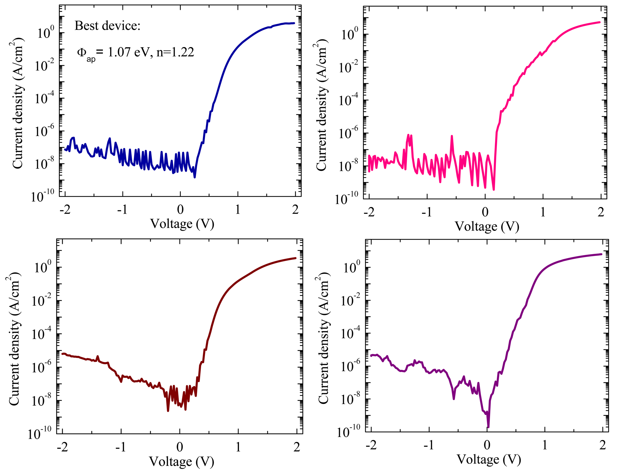
Figure 4 shows the current-voltage (I-V) curves measured at room temperature for four representative Ag/Be0.02Mg0.26ZnO/ZnO Schottky diodes with a Schottky area of 1.1×10⁻⁴ cm2 within one wafer. The forward currents increase exponentially with applied voltage up to 0.25 V, beyond which the voltage drops across the series resistance become apparent. The highest Schottky barrier height of Φap of 1.07 eV was attained with an ideality factor n of 1.22. Rectification ratios of about 1×10⁸ are achieved by using the current values measured at V=±2 V.

Figure 1. Surface characterization. Left column shows the RHEED patterns taken along the [1-100] azimuthal direction during MBE growth of a Be0.02Mg0.26ZnO/ZnO heterostructure, and right column presents the surface morphologies of the GaN template, HT-ZnO layer, and Be0.02Mg0.26ZnO layer measured by AFM. LT-ZnO buffer technology enables the 2D-mode growth of high-quality ZnO heterostructures on low lattice-mismatched GaN templates. Please click here to view a larger version of this figure.

Figure 2. HRXRD of the heterostructure. HRXRD triple-axis 2θ-ω scan of a typical Zn-polar Be0.02Mg0.26ZnO/ZnO heterostructure with a 50 nm thick Be0.02Mg0.26ZnO barrier layer . The reflections at 34.46 o, 34.54 o, and 34.75 o are consistent with (0002) reflections of ZnO, GaN, and Be0.02Mg0.26ZnO, respectively. Please click here to view a larger version of this figure.

Figure 3. Electronic Properties of the heterostructure. Temperature dependences of sheet carrier density and electron mobility of a Zn-polar Be0.02Mg0.26ZnO/ZnO heterostructure. Please click here to view a larger version of this figure.

Figure 4. Schottky diodes. Typical I-V characteristics of four representative Ag/Be0.02Mg0.26ZnO/ZnO Schottky diodes measured at room-temperature. The similarity of the four I-V curves indicates the high in-wafer uniformity of the sample. Please click here to view a larger version of this figure.
Discussion
Incorporation of BeO into MgZnO to form the quaternary BeMgZnO provides the feasibility to tune the extent and sign of strain in the quaternary and hence significantly increases the 2DEG density8. The representative results show that the Be0.02Mg0.26ZnO/ZnO heterostructure results in a 2DEG density close to the desired plasmon-LO phonon resonance electron density (~7×1012 cm-2)24. Although the electron mobility of the heterostructure strongly depends on the MBE growth parameters such as the substrate temperature and VI/II ratio of both the HT-ZnO and the BeMgZnO barrier layer, the 2DEG density is weakly dependent on the growth conditions and mainly determined by the Be and Mg content in the barrier.
A GaN template is used for the growth of BeMgZnO/ZnO heterostructures with high crystalline quality owing to the moderate lattice mismatch of 1.8% between GaN and ZnO, compared with a large lattice mismatch of 18% between sapphire and ZnO. To avoid any conductive parallel channel, it is critical to have a high resistance in the MΩ/square range for the GaN template. In our case, this is achieved by growing at a low chamber pressure of 76 Torr to enhance carbon compensation. To ensure the polarity control in the BeMgZnO/ZnO heterostructures (Zn-polarity), careful surface treatment of GaN template is indispensable. Any oxidation or contamination introduced during the preparation on the GaN surface would induce Zn- and O- mix-polarity in the heterostructures even the determinant VI/II ratio <1.5 is fulfilled.
Any chemical reaction between the metal and the semiconductor, the presence of surface contaminants, states, defects in the vicinity of the surface, and the diffusion of metal into the semiconductor are common problems in the field of the fabrication of Schottky contacts. A variety of methods has been reported in the literature for preparing the surface of ZnO for Schottky contact fabrication. Among them are etching in HCl (or other acids), physical etching with Ar+, UV Ozone cleaning, treatment in H2O2, and O2 plasma (or mixture with He)25,26,27,28. The etching procedures aim for the removal of a surface layer with thickness a ranging from a few nanometers to microns and therefore cannot be applied for HFET devices. The UV-Ozone cleaning or O2 plasma procedure removes only the surface layer. Therefore, it is well suited for the surface preparation of our BeMgZnO/ZnO heterostructures.
Usually Schottky contacts are achieved by depositing a high work function metal such as Pd, Pt, Ir, etc. In contrast, Ag has a low work function of 4.26 eV. Despite that, devices utilizing Ag electrode can show rectifying behavior owing to the formation of an interface silver oxide layer caused by partial oxidation of Ag with oxygen from ZnO matrix. The so formed oxide layer is transparent for electrons and has higher work function compared to Ag. Raju et al. have reported work functions around 5.5 eV for AgO grown by pulsed laser deposition (PLD), which is 1.3 eV higher than that of Ag, and close to the characteristic of Pd, Pt, and Ir29. Our results indicate that that Ag electrode (with O2 plasma pretreatment on the surface of ZnO heterostructure) is a promising contact metal for the formation of Schottky diodes.
We have demonstrated a method for fabricating high quality Schottky contacts for ZnO-based HFETs. MOCVD grown GaN template with careful surface preparation just prior to MBE growth and a low VI/II ratio <1.5 during ZnO nucleation ensure the Zn-polar orientation of the ZnO-based heterostructures with high quality. MOCVD is a widely-used mature technique for epitaxy of GaN for various applications. The MBE procedure described in this work indicates the combinability of MOCVD and MBE techniques, and GaN and oxide semiconductors for electronic devices. Incorporation of a small amount of Be into the BeMgZnO barrier layer results in HFETs with high 2DEG density, high electron mobility, and high thermal stability, for enhanced high speed performance.
Disclosures
The authors have nothing to disclose.
Acknowledgements
This work was supported by Air Force Office of Scientific Research (AFOSR) under Grant FA9550-12-1-0094.
Materials
| Name | Company | Catalog Number | Comments |
| MOCVD | Emcore | custom-built | |
| MBE | SVT Associates | ||
| TMAl | SAFC | CAS: 75-24-1 | |
| TMGa | SAFC | CAS: 1445-79-0 | |
| NH3 | The Linde group | CAS: 7664-41-7 | |
| H2 | National Welders Supply Co. | supplier part no. 335-041 | Grade 5.0 |
| O2 | National Welders Supply Co. | supplier part no. OX 300 | Industrial Grade Oxygen, Size 300 Cylinder, CGA-540 |
| Mg | Sigma-Aldrich | Product No.: 474754-25G | MAGNESIUM, DISTILLED, DENDRITIC PIECES, 99.998% METALS BASIS |
| Be | ESPI Metals | Stock No. K646b | Beryllium pieces, 3N |
| Zn | Alfa Aesar, Thermo Fisher Scientific Chemicals Inc. | Product No.: 10760-30 | Zinc shot, 1-6mm (0.04-0.24in), Puratronic, 99.9999% |
| Au | Kurt J. Lesker | part no. EVMAUXX40G | Gold Pellets, 99.99% |
| Ag | Kurt J. Lesker | part no. EVMAG40QXQ | Silver Pellets, 99.99% |
| Ti | Kurt J. Lesker | part no. EVMTI45QXQ | Titanium Pellets, 99.995% |
| Developer | Rohm and Haas electronic Materials LLC | MF-CD-26 | Material number 10018050 |
| Photoresist | Rohm and Haas electronic Materials LLC | SPR 955 | Material number 10018283 |
References
- Morkoc, H., Solomon, P. M. The hemt: A superfast transistor: An experimental GaAs-AlGoAs device switches in picoseconds and generates little heat. This is just what supercomputers need. IEEE spectrum. 21 (2), 28-35 (1984).
- Aktas, O., et al. Microwave performance of AlGaN/GaN inverted MODFET's. IEEE Electron Device Letters. 18 (6), 293-295 (1997).
- Leach, J. H., et al. Effect of hot phonon lifetime on electron velocity in InAlN/AlN/GaN heterostructure field effect transistors on bulk GaN substrates. Applied Physics Letters. 96 (13), 133505 (2010).
- Sasa, S., et al. Microwave performance of ZnO/ZnMgO heterostructure field effect transistors. Physica status solidi (a). 208 (2), 449-452 (2011).
- Ye, D., et al. Enhancement-mode ZnO/Mg0.5Zn0.5O HFET on Si. Journal of Physics D: Applied Physics. 47 (25), 255101 (2014).
- Koike, K., et al. Molecular beam epitaxial growth of wide bandgap ZnMgO alloy films on (111)-oriented Si substrate toward UV-detector applications. Journal of Crystal Growth. 278 (1-4), 288-292 (2005).
- Du, X., et al. Controlled Growth of High-Quality ZnO-Based Films and Fabrication of Visible-Blind and Solar-Blind Ultra-Violet Detectors. Advanced Materials. 21 (45), 4625-4630 (2009).
- Ding, K., Ullah, M., Avrutin, V., Özgür, &. #. 2. 2. 0. ;., Morkoç, H. Investigation of high density two-dimensional electron gas in Zn-polar BeMgZnO/ZnO heterostructures. Applied Physics Letters. 111 (18), 182101 (2017).
- Ding, K., Avrutin, V., Özgür, &. #. 2. 2. 0. ;., Morkoç, H. III-Nitride Light-Emitting Diodes. Wiley Encyclopedia of Electrical and Electronics Engineering. , 1-21 (2017).
- Tsukazaki, A., et al. Quantum Hall effect in polar oxide heterostructures. Science. 315 (5817), 1388-1391 (2007).
- Tsukazaki, A., et al. Observation of the fractional quantum Hall effect in an oxide. Nat Mater. 9 (11), 889-893 (2010).
- Falson, J., et al. MgZnO/ZnO heterostructures with electron mobility exceeding 1 x 10(6) cm(2)/Vs. Sci Rep. 6, 26598 (2016).
- Ullah, M. B., et al. Polarity control and residual strain in ZnO epilayers grown by molecular beam epitaxy on (0001) GaN/sapphire. physica status solidi (RRL) Rapid Research Letters. 10 (9), 682-686 (2016).
- Ullah, M. B., et al. Characterization of Ag Schottky Barriers on Be0.02Mg0.26ZnO/ZnO Heterostructures. physica status solidi (RRL) - Rapid Research Letters. , (2017).
- Lee, J. H., et al. Schottky diodes prepared with Ag, Au, or Pd contacts on a MgZnO/ZnO heterostructure. Japanese Journal of Applied Physics. 51 (9S2), 09MF07 (2012).
- Singh, R., et al. Investigation of barrier inhomogeneities and interface state density in Au/MgZnO: Ga Schottky contact. Journal of Physics D: Applied Physics. 49 (44), 445303 (2016).
- Brillson, L. J., Lu, Y. ZnO Schottky barriers and Ohmic contacts. Journal of Applied Physics. 109 (12), 121301 (2011).
- Müller, S., et al. Method of choice for fabrication of high-quality ZnO-based Schottky diodes. Journal of Applied Physics. 116 (19), 194506 (1945).
- Figge, S., Böttcher, T., Einfeldt, S., Hommel, D. In situ and ex situ evaluation of the film coalescence for GaN growth on GaN nucleation layers. Journal of Crystal Growth. 221 (1-4), 262-266 (2000).
- Han, J., Ng, T. -. B., Biefeld, R., Crawford, M., Follstaedt, D. The effect of H 2 on morphology evolution during GaN metalorganic chemical vapor deposition. Applied Physics Letters. 71 (21), 3114-3116 (1997).
- Berger, H. Models for contacts to planar devices. Solid-State Electronics. 15 (2), 145-158 (1972).
- Tampo, H., et al. Polarization-induced two-dimensional electron gases in ZnMgO/ZnO heterostructures. Applied Physics Letters. 93 (20), 202104 (2008).
- Ye, J. D., et al. Two-dimensional electron gas in Zn-polar ZnMgO/ZnO heterostructure grown by metal-organic vapor phase epitaxy. Applied Physics Letters. 97 (11), 111908 (2010).
- Šermukšnis, E., et al. Hot-electron energy relaxation time in Ga-doped ZnO films. Journal of Applied Physics. 117 (6), 065704 (2015).
- Singh, C., Agarwal, G., Rao, G. D., Chaudhary, S., Singh, R. Effect of hydrogen peroxide treatment on the electrical characteristics of Au/ZnO epitaxial Schottky diode. Materials Science in Semiconductor Processing. 14 (1), 1-4 (2011).
- Mohanta, S., et al. Electrical characterization of Schottky contacts to n-MgZnO films. Thin Solid Films. 548, 539-545 (2013).
- Schifano, R., Monakhov, E., Grossner, U., Svensson, B. Electrical characteristics of palladium Schottky contacts to hydrogen peroxide treated hydrothermally grown ZnO. Applied Physics Letters. 91 (19), 193507 (2007).
- Ip, K., et al. Improved Pt/Au and W/Pt/Au Schottky contacts on n-type ZnO using ozone cleaning. Applied Physics Letters. 84 (25), 5133-5135 (2004).
- Raju, N. R. C., Kumar, K. J., Subrahmanyam, A. Physical properties of silver oxide thin films by pulsed laser deposition: effect of oxygen pressure during growth. Journal of Physics D: Applied Physics. 42 (13), 135411 (2009).
Reprints and Permissions
Request permission to reuse the text or figures of this JoVE article
Request PermissionExplore More Articles
This article has been published
Video Coming Soon
Copyright © 2025 MyJoVE Corporation. All rights reserved