Method Article
Rendering SiO2/Si Surfaces Omniphobic by Carving Gas-Entrapping Microtextures Comprising Reentrant and Doubly Reentrant Cavities or Pillars
In This Article
Summary
This work presents microfabrication protocols for achieving cavities and pillars with reentrant and doubly reentrant profiles on SiO2/Si wafers using photolithography and dry etching. Resulting microtextured surfaces demonstrate remarkable liquid repellence, characterized by robust long-term entrapment of air under wetting liquids, despite the intrinsic wettability of silica.
Abstract
We present microfabrication protocols for rendering intrinsically wetting materials repellent to liquids (omniphobic) by creating gas-entrapping microtextures (GEMs) on them comprising cavities and pillars with reentrant and doubly reentrant features. Specifically, we use SiO2/Si as the model system and share protocols for two-dimensional (2D) designing, photolithography, isotropic/anisotropic etching techniques, thermal oxide growth, piranha cleaning, and storage towards achieving those microtextures. Even though the conventional wisdom indicates that roughening intrinsically wetting surfaces (θo < 90°) renders them even more wetting (θr < θo < 90°), GEMs demonstrate liquid repellence despite the intrinsic wettability of the substrate. For instance, despite the intrinsic wettability of silica θo ≈ 40° for the water/air system, and θo ≈ 20° for the hexadecane/air system, GEMs comprising cavities entrap air robustly on immersion in those liquids, and the apparent contact angles for the droplets are θr > 90°. The reentrant and doubly reentrant features in the GEMs stabilize the intruding liquid meniscus thereby trapping the liquid-solid-vapor system in metastable air-filled states (Cassie states) and delaying wetting transitions to the thermodynamically-stable fully-filled state (Wenzel state) by, for instance, hours to months. Similarly, SiO2/Si surfaces with arrays of reentrant and doubly reentrant micropillars demonstrate extremely high contact angles (θr ≈ 150°–160°) and low contact angle hysteresis for the probe liquids, thus characterized as superomniphobic. However, on immersion in the same liquids, those surfaces dramatically lose their superomniphobicity and get fully-filled within <1 s. To address this challenge, we present protocols for hybrid designs that comprise arrays of doubly reentrant pillars surrounded by walls with doubly reentrant profiles. Indeed, hybrid microtextures entrap air on immersion in the probe liquids. To summarize, the protocols described here should enable the investigation of GEMs in the context of achieving omniphobicity without chemical coatings, such as perfluorocarbons, which might unlock the scope of inexpensive common materials for applications as omniphobic materials. Silica microtextures could also serve as templates for soft materials.
Introduction
Solid surfaces that exhibit apparent contact angles, θr > 90° for polar and nonpolar liquids, such as water and hexadecane, are referred to as omniphobic1. These surfaces serve numerous practical applications, including water desalination2,3, oil-water separation4,5, antibiofouling6, and reducing hydrodynamic drag7. Typically, omniphobicity necessitates perfluorinated chemicals and random topographies8,9,10,11,12. However, the cost, non-biodegradability, and vulnerability of those materials/coatings pose a myriad of constraints, e.g., perfluorinated desalination membranes degrade as the feed-side temperatures are raised, leading to pore-wetting13,14, and perfluorinated/hydrocarbon coatings also get abraded15,16 and degraded by silt particles in the flow streams and cleaning protocols. Thus, there is a need for alternative strategies for achieving the functions of perfluorinated coatings (i.e., entrapping air on immersion in liquids without using water repellent coatings). Therefore, researchers have proposed surface topographies comprised of overhanging (reentrant) features that could entrap air on immersion by microtexturing alone17,18,19,20,21,22,23,24,25. These microtextures come in three types: cavities26, pillars27, and fibrous mats8. Hereafter, we will refer to reentrant features with simple overhangs as reentrant (Figure 1A–B and Figure 1E–F) and reentrant features with overhangs that make a 90°-turn towards the base as doubly reentrant (Figure 1C–D and Figure 1G–H).
In their pioneering work, Werner et al.22,28,29,30,31 characterized cuticles of springtails (Collembola), soil-dwelling arthropods, and explained the significance of mushroom-shaped (reentrant) features in the context of wetting. Others have also investigated the role of mushroom-shaped hairs in sea-skaters32,33 towards facilitating extreme water repellence. Werner and coworkers demonstrated the omniphobicity of intrinsically wetting polymeric surfaces by carving biomimetic structures through reverse imprint lithography29. Liu and Kim reported on silica surfaces adorned with arrays of doubly reentrant pillars that could repel drops of liquids with surface tensions as low as γLV = 10 mN/m, characterized by apparent contact angles, θr ≈ 150° and extremely low contact angle hysteresis27. Inspired by these amazing developments, we followed the recipes of Liu and Kim to reproduce their results. However, we discovered that those microtextures would catastrophically lose their superomniphobicity, i.e. θr → 0°, if wetting liquid drops touched the edge of the microtexture or if there was localized physical damage34. These findings demonstrated that pillar-based microtextures were unfit for applications that required omniphobicity on immersion, and they also questioned the criteria for assessing omniphobicity (i.e., should they be limited to contact angles alone, or if additional criteria are needed).
In response, using the SiO2/Si wafers, we prepared arrays of microscale cavities with doubly reentrant inlets and, and using water and hexadecane as the representative polar and nonpolar liquids, we demonstrated that (i) these microtextures prevent liquids from entering them by entrapping air, and (ii) the compartmentalized architecture of the cavities prevents the loss of the entrapped air by localized defects34. Thus, we have termed these microtextures as "gas-entrapping microtextures" (GEMs). As the next step, we microfabricated GEMs with varying shapes (circular, square, hexagonal) and profiles (simple, reentrant, and doubly reentrant) to systematically compare their performance under immersion in wetting liquids26. We also created a hybrid microtexture comprising arrays of doubly reentrant pillars surrounded by walls with doubly reentrant profiles, which prevented liquids from touching the stems of the pillars and robustly entrapped air on immersion35. Below, we present detailed protocols for manufacturing GEMs on SiO2/Si surfaces through photolithography and etching techniques along with design parameters. We also present representative results of characterizing their wetting by contact angle goniometry (advancing/receding/as-placed angles) and immersion in hexadecane and water.
Protocol
NOTE: Arrays of reentrant and doubly reentrant cavities and pillars were microfabricated by adapting the multistep protocol for pillars reported by Liu and Kim27. Precautions were taken to minimize the formation of pin residues or particles on our surfaces that could interfere with wetting transitions36.
MICROFABRICATION OF CAVITIES
Broadly, the protocols for the microfabrication of reentrant and doubly reentrant cavities (RCs and DRCs) consist of two-dimensional layout designing, photolithography, general silica etching, and specific silicon etching, depending on the final feature required37,38,39,40,41.
1. Design
- Start the microfabrication process by designing the required pattern in a layout software42. An example of such a software is listed in the Materials List.
- Using the software, create a new file. Draw a unit cell comprising a circle of diameter, D = 200 µm. Copy and paste this circle with a center-to-center distance (pitch) of L = 212 µm to create an array of circles in a square patch of area 1 cm2 (Figure 2).
- Draw a circle of diameter 100 mm (4 inches). Place the 1 cm2 square array inside the circle and replicate it to create a 4 x 4 grid of square arrays. Features inside the circle will be transferred onto the 4-inch wafers (Figure 2).
- Export the design file to the desired format for the mask writing system (e.g., the GDSII format).
2. Cleaning of Wafers
- Clean a silicon wafer 4 inches in diameter, <100> orientation, and with a 2.4 µm thick thermal oxide layer (see the Materials List), in piranha solution for 10 min. Piranha solution comprises sulfuric acid (H2SO4, 96%): hydrogen peroxide (H2O2, 30%) in a 3:1 volumetric ratio and is maintained at T = 388 K.
- Rinse the wafer with deionized water and spin-dry under nitrogen (N2) environment.
3. Photolithography
- Coat the wafer with hexamethyldisilazane (HMDS) using vapor-phase deposition to improve adhesion with the photoresist. Refer to Table 1 for the process details.
- Mount the wafer on a 4-inch vacuum chuck in the spin coater. Cover the wafer with the AZ-5214E photoresist. Use the spin coater to spread the photoresist uniformly on the surface as a 1.6 µm-thick layer. Refer to Table 2 for spin coating parameters.
- Bake the photoresist-coated wafer on a hot-plate maintained at 110 °C for 120 s.
- Transfer the wafer to a direct-writing system and expose the wafer to UV radiation for 55 ms (defocus: +5). This step transfers the desired design on the AZ-5214E (used in the positive tone; see Materials List) (Figure 2).
- Place the UV-exposed wafer in a glass Petri dish containing the AZ-726 developer for 60 s for the features to develop. See Materials List for details.
- Remove the wafer from the developer solution and rinse with deionized (DI) water gently to remove excess developer. Spin dry the wafer in a N2 environment. These steps are presented in Figure 3A–C.
NOTE: At the end of this step, design patterns on the wafer can be seen under a standard optical microscope.
4. Anisotropic Etching of Silica (SiO2) Layer
NOTE: The goal of this step is to completely etch away the silica layer (2.4 µm-thick) that was exposed during photolithography to expose the silicon layer underneath.
- After photolithography, transfer the wafer to an inductively coupled plasma (ICP) reactive-ion etching (RIE) system that employs a mixture of octafluorocyclobutane (C4F8) and oxygen (O2) gases to etch silica vertically downward (anisotropic etching).
- Run the ICP-RIE process for approximately 13 min to etch the exposed silica layer. Refer to the ICP-RIE parameters in Table 3. During this step, the photoresist layer also gets completely etched away (Figure 3C–D).
- To ensure that the silica layer thickness inside the desired patterns is reduced to zero, so that the silicon layer is exposed, measure the thickness of the remaining silica using a reflectometer. Adjust the duration of the subsequent etching period based on the thicknesses of the silica layers (especially in and around the patterns).
NOTE: A reflectometer was used to measure the thickness of the remaining silica layer43. Alternatively, other tools, such as ellipsometer or an interactive color chart to predict the color of SiO2 and thickness can also be used44,45.
The procedures detailed in steps 1 and 4 are common for both reentrant and doubly reentrant cavities. However, the etching protocols for the silicon layer are different and are described below:
5. Reentrant Cavities
- Anisotropic silicon etching
- After etching the silica layer, transfer the wafer to a deep ICP-RIE system to etch silicon. The first step consists of a fluorine-based anisotropic etching method known as the Bosch process that etches silicon vertically downward, creating a straight wall.
NOTE: The Bosch process uses C4F8 and sulfur hexafluoride (SF6) gases in the reaction chamber: the C4F8 deposition creates a passivation layer, while the SF6 etches silicon vertically downward. Thus, the Bosch process enables the microfabrication of deep trenches in silicon with high-aspect ratios. - Run this process for five cycles, which corresponds to an etching depth for silicon equivalent to ≈ 2 µm. Process parameters are listed in Table 4.
- Clean the wafer in piranha solution for 10 min to remove any remnants of the Bosch process. Rinse the wafer with DI water and spin-dry in a N2 environment (Figure 3E).
- After etching the silica layer, transfer the wafer to a deep ICP-RIE system to etch silicon. The first step consists of a fluorine-based anisotropic etching method known as the Bosch process that etches silicon vertically downward, creating a straight wall.
- Isotropic silicon etching: In order to create the reentrant feature, perform isotropic etching that would create an undercut beneath the silica layer. A 5 µm overhang can be achieved by etching the silicon layer with SF6 for 2 min 45 s (Figure 3F). Refer to Table 5 for the process parameters.
- Anisotropic silicon etching: Once the reentrant features are created, tune the depth of the cavities by the Bosch process (step 5.1).
NOTE: To microfabricate cavities with a depth of hc ≈ 50 µm, 160 cycles of the Bosch process are required (Figure 3G, Table 4). - Wafer cleaning and storage
- Clean the wafer using piranha solution as described in step 2. After this step, the wafer becomes superhydrophilic, characterized by contact angles of water, θo ≈ 0°.
- Store the wafer in a glass Petri dish and place inside a clean vacuum oven maintained at T = 323 K and vacuum pressure PVac = 3.3 kPa for 48 h, after which the intrinsic contact angle of the silica layer stabilizes to θo ≈ 40°.
- Store the samples in a clean cabinet equipped with an outward nitrogen (99%) flow, ready for further characterization.
6. Doubly Reentrant Cavities
- Anisotropic silicon etching: To create doubly reentrant cavities, follow steps 1, 2, 3, 4, and 5.1 (see Figure 4A–E).
- Isotropic silicon etching
In order to create doubly reentrant features, reentrant features must be created first. To achieve that, perform isotropic etching to create an undercut beneath the silica layer. Etch the silicon layer with SF6 for 25 s (Figure 4F). Refer to Table 5 for the process parameters. Subsequently, clean the wafer using piranha solution as described in step 2. - Thermal oxide growth
- To achieve doubly reentrant features, grow a 500 nm layer of thermal oxide on the wafer, using a high temperature furnace system (Figure 4G).
- Measure the thickness of the oxide layer using a reflectometer.
NOTE: The oxidation was carried out by exposing the samples to an environment comprising oxygen (O2) and water vapor, leading to the wet oxidation of silicon in an enclosed environment at temperatures ranging from 800–1,200 °C.
- Silica etching: Carry out the same process as described in the step 4 to etch silica vertically downward for 3 min. As a result of the anisotropic etching, the thermal oxide (500 nm thick silica layer) is etched away from the cavity, but it leaves an "overhang" along the sidewalls that would form the doubly reentrant edge eventually (Figure 4H, Table 3).
- Anisotropic silicon etching: Repeat five cycles of the Bosch process to deepen of the cavities by ≈ 2 µm (Figure 4I, Table 5). This step is necessary to remove the silicon behind the doubly reentrant feature in the next step. Clean the wafer using piranha solution.
- Isotropic silicon etching: Perform the isotropic etching of silicon for 2 min and 30 s using the process parameters described in Table 4. This step creates an empty space (≈2 µm) behind the thermally-grown oxide at the mouth of the cavity, leading to the doubly reentrant edge (Figure 4J).
- Anisotropic silicon etching: Use the Bosch process recipe (step 5.1) for 160 cycles to increase the depth of the cavities to hc ≈ 50 µm, (Figure 4K, Table 5).
- Wafer cleaning and storage: Clean the wafer using piranha solution and store as described in step 5.4 above.
MICROFABRICATION OF PILLARS
The design protocol for fabricating reentrant and doubly reentrant pillars and "hybrids" (comprising doubly reentrant pillars surrounded by walls) consists of three key steps: wafer preparation, silica etching, and specific silicon etching. Figure 5A–C show the top-view of the layout design for reentrant and doubly reentrant pillars, while Figure 5D–F represent the layout of the hybrid arrays. Select the dark-field option of the UV exposure in order to expose the whole wafer except for the pattern using the same photoresist (AZ5214E) (Figure 6A–C and Figure 7A–C). Besides these specificities, the processes for cleaning the wafer (step 2) and etching silica (step 4) are identical.
7. Reentrant Pillars
- Anisotropic silicon etching: After photolithography, UV exposure, development, and etching silica with the specificities for pillars described above (steps 1–4), transfer the wafer to a deep ICP-RIE system to etch the silicon layer using the Bosch process. This step controls the height of the pillars. Use 160 cycles of the Bosch process to achieve pillars of height, hP ≈ 30 µm (Figure 6E, Table 5). Clean the wafer as described in step 2.
- Isotropic silicon etching: Perform isotropic etching using SF6 for 5 min to create the reentrant edge on the pillars (Figure 6F, Table 4). The resulting length of the overhang is 5 µm.
- Piranha cleaning and storage: Clean the wafer using piranha solution and store as described in step 5.4 above.
8. Doubly Reentrant Pillars and Hybrids
- Anisotropic silicon etching: After etching SiO2, transfer the wafer to a deep ICP-RIE system to etch the Si under the SiO2 layer. Perform five cycles of the Bosch process that corresponds to an etching depth of ≈ 2 µm (Figure 7E, Table 4). Subsequently, clean the wafer as described in step (2).
- Isotropic silicon etching: Carry out isotropic etching using SF6 for 16 s to create the reentrant edge (Table 5, Figure 7F). Clean the wafer as described in step 2.
- Thermal oxide growth: Grow 500 nm layer of thermal oxide all over the wafer using a high temperature furnace system as described in step 6.3 (Figure 7G).
- Silica etching: Etch the thermally-grown oxide layer (500 nm thick) for 3 min as described in step 6.4 (Figure 7H, Table 3).
- Anisotropic silicon etching: Repeat 160 cycles of the Bosch process (Table 4) to increase the height of the pillars (Figure 7I). Clean the wafer as described in step 2 above.
- Isotropic silicon etching: Perform isotropic etching of silicon for 5 min using the process parameters as described in Table 4. This step creates the doubly reentrant edge (Figure 7J). The space between pillar stem and doubly reentrant edge is ≈2 µm.
- Wafer cleaning and storage: Clean the wafer using piranha solution and store as described in step 5.4 above.
Figure 8 represents the list of processes used in microfabricating reentrant and doubly reentrant cavities and pillars.
Results
In this section, we showcase reentrant and doubly reentrant cavities (RCs and DRCs, Figure 9) and reentrant and doubly reentrant pillars (RPs and DRPs, Figure 10) microfabricated using the protocols described above. All the cavities have the diameter, DC = 200 μm, the depth, hC ≈ 50 μm, and the center-to-center distance (or the pitch) between adjacent cavities to be LC = DC + 12 μm. Using the same fabrication protocols, cavities of non-circular shapes can also be prepared, as reported previously26.
The diameter of the cap on top of the pillars was DP = 20 μm, and their height and pitch were, respectively, hp ≈ 30 μm and LP = 100 μm (Figure 10).
Wetting Behaviors of Gas-Entrapping Microtextures (GEMs)
Flat silica (SiO2) is intrinsically wetting towards most polar and nonpolar liquids. For instance, the intrinsic contact angles of droplets of hexadecane (γLV = 20 mN/m at 20 °C) and water (surface tension γLV = 72.8 mN/m at 20 °C) on silica were, respectively, and θo ≈ 20° and θo ≈ 40°. However, after microfabricating reentrant and doubly reentrant cavities (DRCs) and pillars, the contact angles changed dramatically (Table 6). We measured the advancing/receding contact angles by dispensing/retracting the liquids at the rate of 0.2 µL/s and found the apparent contact angles for both liquids, θr > 120°, (omniphobic; Figure 11E). Receding contact angles, θr ≈ 0° because of the lack of discontinuity in the microtextures, such as in pillar-based microtextures. On the other hand, SiO2/Si surfaces with arrays of doubly reentrant pillars (DRPs) exhibited apparent contact angles, θr > 150° for both liquids and the contact angle hysteresis was minimal (superomniphobic, Figure 11A and Movies S1 and S2). Curiously, when the same SiO2/Si surfaces with arrays of pillars were immersed in the same liquids they got intruded instantaneously, t < 1 s, i.e. no air was entrapped (Figure 10A–D, Movie S3). So, while the pillars appeared to be superomniphobic in terms of contact angles, they failed to entrap air on immersion. In fact, wetting liquids intrude from the boundary of the microtexture (or from localized defects) and displace any trapped air instantaneously (Figure 11A–D and Movie S3). In contrast, DRCs entrapped air upon immersion in both liquids (Figure 11E–H and S1, Table 1); for hexadecane, the entrapped air was intact even after 1 month26. Our confocal microscopy experiments demonstrated that the overhanging features stabilize the intruding liquids and entrap air inside them (Figure 12A–B).
Next, to entrap air in arrays of DRPs, we employed the same microfabrication protocols to achieve arrays of pillars surrounded by walls of doubly reentrant profile (Figure 10G–I). This strategy insulated the stems of the DRPs from wetting liquids. As a result, the hybrid microtextures behaved as GEMs, as confirmed by confocal microscopy (Figure 12C–D) and Movie S4, Table 6). Thus, silica surfaces with hybrid microtextures exhibited omniphobicity on immersion by trapping air and demonstrated contact angles, θr > 120°, (omniphobic), and proved omniphobic in the true sense, i.e. in terms of contact angles and entrapping air on immersion. In Table 6, we assess the omniphobicity of SiO2/Si surfaces with a variety of microtextures cavity-based, pillar-based, and hybrids by contact angles and immersion.
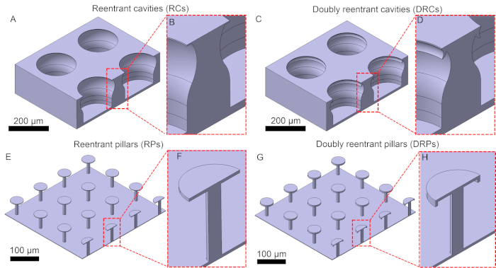
Figure 1: Schematics of microstructures. (A–B) Reentrant cavities, (C–D) doubly reentrant cavities, (E–F) reentrant pillars, (G–H) doubly reentrant pillars. Please click here to view a larger version of this figure.
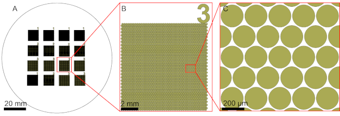
Figure 2: Design patterns for cavities. Design patterns for reentrant and doubly reentrant cavities generated using the layout software. The pattern was transferred onto the wafer using photolithography. Please click here to view a larger version of this figure.

Figure 3: Microfabrication protocol for reentrant cavities. (A) Clean silicon wafer with 2.4 µm thick silica on top. (B) Spin-coat the wafer with photoresist and expose to UV light. (C) Develop the UV exposed photoresist to obtain the design pattern. (D) Etching of the exposed top silica layer vertically downward (anisotropic etching) using inductively coupled plasma (ICP) reactive-ion etching (RIE). (E) Shallow anisotropic etching of exposed silicon layer using deep ICP-RIE. (F) Isotropic etching of silicon to create the reentrant edge. (G) Deep anisotropic silicon etching to increase the depth of the cavities. Please click here to view a larger version of this figure.
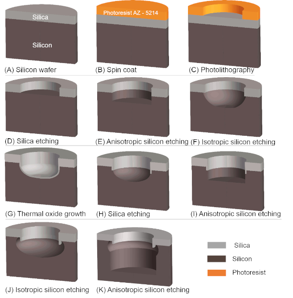
Figure 4: Microfabrication protocol for doubly reentrant cavities. (A) Clean silicon wafer with 2.4 µm thick silica on top. (B) Spin-coat the wafer with photoresist and expose to UV light. (C) Develop the UV exposed photoresist to obtain the design pattern. (D) Etching of the exposed top silica layer vertically downward (anisotropic etching) using inductively coupled plasma (ICP) reactive-ion etching (RIE). (E) Shallow anisotropic etching of exposed silicon layer using deep ICP-RIE. (F) Shallow isotropic etching of silicon to create undercut using deep ICP-RIE. (G) Thermal oxide growth. (H) Anisotropic etching of top and bottom silica layer. (I) Shallow anisotropic etching of silicon. (J) Isotropic silicon etch to create the doubly reentrant edge. (K) Deep anisotropic silicon etching to increase the depth of the cavities. Please click here to view a larger version of this figure.
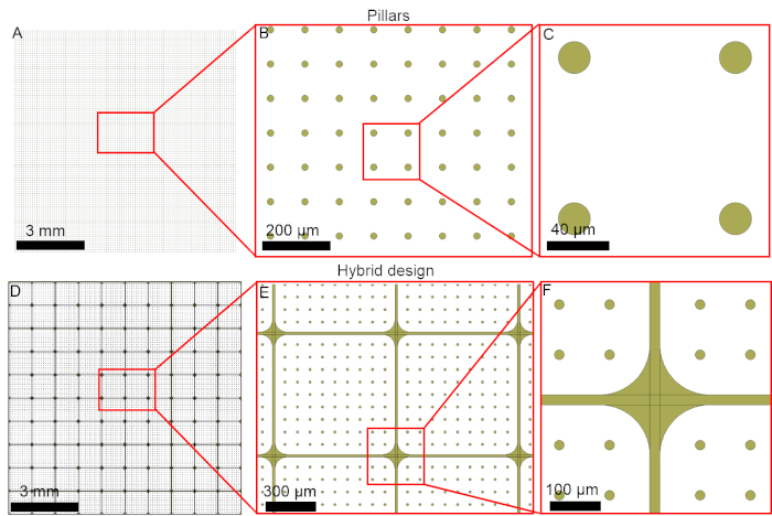
Figure 5: Design patterns for pillars. Design patterns for reentrant, doubly reentrant, and hybrid pillars generated using the layout software. The pattern was transferred onto the wafer using photolithography. Please click here to view a larger version of this figure.
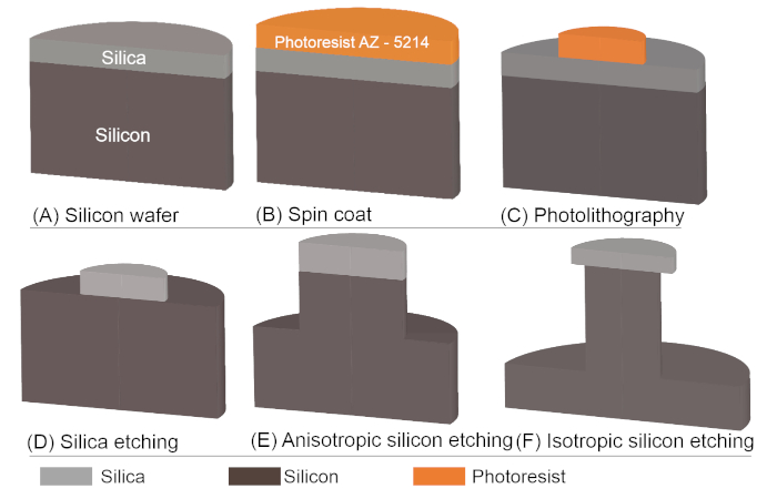
Figure 6: Microfabrication protocol of reentrant pillars. (A) Clean silicon wafer with 2.4 µm thick silica on top. (B) Spin-coat the wafer with photoresist and expose to UV light. (C) Develop the UV exposed photoresist to obtain the design pattern. (D) Etching of the exposed top silica layer vertically downward (anisotropic etching) using inductively coupled plasma (ICP) reactive-ion etching (RIE). (E) Deep anisotropic silicon etching to increase the height of the pillars. (F) Isotropic silicon etching to create the reentrant edge. Please click here to view a larger version of this figure.
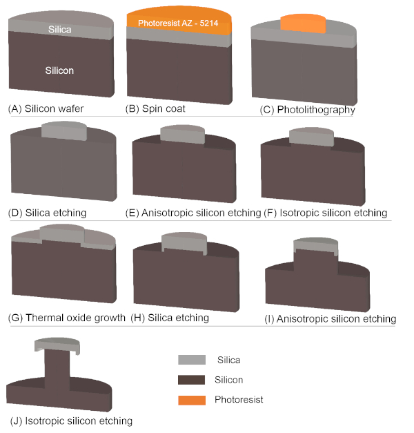
Figure 7: Microfabrication protocol for doubly reentrant pillars. (A) Clean silicon wafer with 2.4 µm thick silica on top. (B) Spin-coat the wafer with photoresist and expose to UV light. (C) Develop the UV exposed photoresist to obtain the design pattern. (D) Etching of the exposed top silica layer vertically downward (anisotropic etching) using inductively coupled plasma (ICP) reactive-ion etching (RIE). (E) Shallow anisotropic etching of exposed silicon layer using deep ICP-RIE. (F) Shallow isotropic etching of silicon to create undercut using deep ICP-RIE. (G) Thermal oxide growth. (H) Anisotropic etching of the top and bottom of silica layer. (I) Anisotropic silicon etching to increase the height of the pillars. (J) Isotropic silicon etching to create the doubly reentrant edge. Note that the only difference between doubly reentrant pillars and the "hybrid" is the design at the beginning. Please click here to view a larger version of this figure.
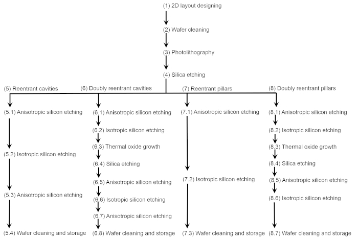
Figure 8: Microfabrication protocol for reentrant and doubly reentrant cavities and pillars. The flowchart lists the key steps involved. Please click here to view a larger version of this figure.
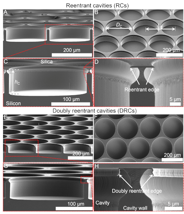
Figure 9: Scanning electron micrographs of reentrant and doubly reentrant cavities. (A–D) Cross sectional and isometric views of silica surfaces with array of reentrant cavities. (E–H) Cross sectional and top views of doubly reentrant cavities. DC = diameter of the cavity and LC = the center-to-center distance between adjacent cavities (or pitch), and hC = depth of the cavity. Please click here to view a larger version of this figure.
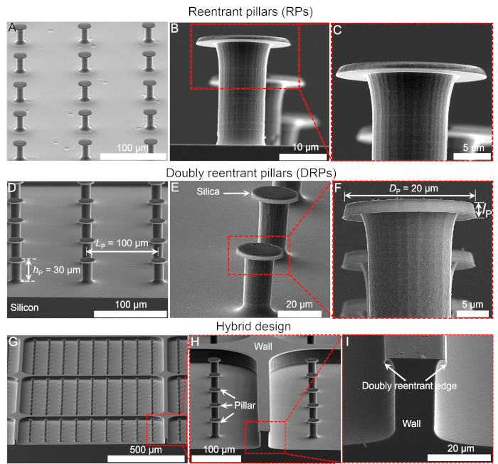
Figure 10: Scanning electron micrographs of reentrant and doubly reentrant pillars. (A–C) Isometric view of reentrant pillars. (D–F) Doubly reentrant pillars. (G–I) Hybrid pillars - DRPs surrounded by doubly reentrant walls. DP - diameter of the pillar cap and LP - the center-to-center distance between adjacent pillars (or pitch), and hP – height of the pillars. Figure D–I, reprinted from Ref.35, Copyright (2019), with permission from Elsevier. Please click here to view a larger version of this figure.

Figure 11: Wetting behavior. (A) Superomniphobicity of SiO2/Si surfaces adorned with arrays doubly reentrant pillars, observed by placing liquid drops on top. (B–D) The superomniphobicity is lost instantaneously, if wetting liquids touch the boundary or localized defects. (E) SiO2/Si surfaces adorned with arrays doubly reentrant cavities exhibit omniphobicity. (F–H) These microtextures entrap air robustly and do not lose it if liquid touches the boundary or localized defects. Reprinted from Ref.35, Copyright (2019), with permission from Elsevier. Please click here to view a larger version of this figure.
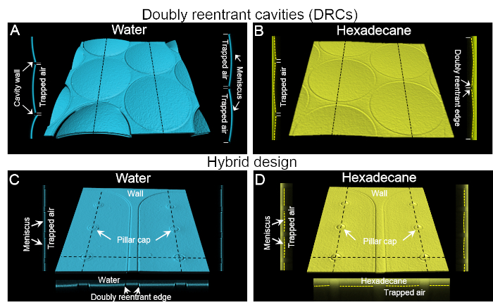
Figure 12: Confocal microscopy of microtextures immersed in liquids. Computer-enhanced 3D reconstructions of representative confocal images (isometric and cross-sections along the dotted lines) of wetting transitions in silica surfaces with doubly reentrant cavities and hybrid pillars immersed under a z ≈ 5 mm column after 5 min of immersion of (A,C) water, and (B,D) hexadecane. The (false) blue and yellow colors correspond to the interfaces of water and hexadecane with the trapped air. Intruding liquid menisci were stabilized at doubly reentrant edge. (Scale bar = Diameter of the cavity and pillar 200 µm and 20 µm respectively). Figure 12 was reprinted from Ref.35, Copyright (2019), with permission from Elsevier. Please click here to view a larger version of this figure.
| Stage 1: Dehydration and purging oxygen from chamber | ||
| Step | Process sequence | Time (min) |
| 1 | Vacuum (10 Torr) | 1 |
| 2 | Nitrogen (760 Torr) | 3 |
| 3 | Vacuum (10 Torr) | 1 |
| 4 | Nitrogen (760 Torr) | 3 |
| 5 | Vacuum (10 Torr) | 1 |
| 6 | Nitrogen (760 Torr) | 3 |
| Stage 2: Priming | ||
| Process sequence | Time (min) | |
| 7 | Vacuum (1 Torr) | 2 |
| 8 | HMDS (6 Torr) | 5 |
| Stage 3: Purging Prime Exhaust | ||
| Process sequence | Time (min) | |
| 9 | Vacuum | 1 |
| 10 | Nitrogen | 2 |
| 11 | Vacuum | 2 |
| Stage 4: Return to Atmosphere (Backfill) | ||
| Process sequence | Time (min) | |
| 12 | Nitrogen | 3 |
Table 1: Process details for coating hexamethyldisilazane (HMDS) layers to enhance the adhesion between the silica surface and the AZ-5214E photoresist.
| Step | Speed (rpm) | Ramp (rpm/s) | Time (s) |
| 1 | 800 | 1000 | 3 |
| 2 | 1500 | 1500 | 3 |
| 3 | 3000 | 3000 | 30 |
Table 2: Process details for achieving 1.6 µm-thick AZ-5214E photoresist layer on SiO2/Si wafers by spin-coating.
| RF power, (W) | ICP power, (W) | Etching pressure, (mTorr) | C4F8 flow (sccm) | O2 flow (sccm) | Temperature, (°C) |
| 100 | 1500 | 10 | 40 | 5 | 10 |
Table 3: Parameter settings for silica etching used in Inductively Coupled Plasma – Reactive Ion Etching (ICP-RIE).
| RF power, (W) | ICP power, (W) | Etching pressure, (mTorr) | SF6 flow, (sccm) | Temperature, (°C) |
| 20 | 1800 | 35 | 110 | 15 |
Table 4: Parameter settings for silicon etching (isotropic) used in inductively coupled plasma – deep reactive ion etching (ICP-DRIE).
| Step | RF power, (W) | ICP power, (W) | Etching pressure, (mTorr) | SF6 flow, (sccm) | C4F8 flow, (sccm) | Temperature, (°C) | Deposition/ Etching time, (s) |
| Passivation layer | 5 | 1300 | 30 | 5 | 100 | 15 | 5 |
| Etching | 30 | 1300 | 30 | 100 | 5 | 15 | 7 |
Table 5: Parameter settings for silicon etching (anisotropic) used in inductively coupled plasma – deep reactive ion etching (ICP-DRIE).
| Surfaces | Criterion: Contact angles in air | Criterion: Immersion | |||
| Water | Hexadecane | Water | Hexadecane | ||
| DRPs | θr | 153°±1° | 153° ± 1° | Instantaneous penetration | Instantaneous penetration |
| θA | 161°±2° | 159° ± 1° | |||
| θR | 139°±1° | 132° ± 1° | |||
| Assessment: | Superomniphobic | Not omniphobic – in fact, omniphilic | |||
| DRCs | θr | 124° ± 2° | 115° ± 3° | Trapped air (omniphobic) | Trapped air (omniphobic) |
| θA | 139° ± 3° | 134° ± 5° | |||
| θR | 0° | 0° | |||
| Assessment: | Omniphobic | Omniphobic | |||
| Hybrids | θr | 153°± 2° | 153° ± 2° | Trapped air (omniphobic) | Trapped air (omniphobic) |
| θA | 161°± 2° | 159° ± 2° | |||
| θR | 0° | 0° | |||
| Assessment: | Omniphobic | Omniphobic | |||
Table 6: Contact angle measurements – advancing (θA), receding (θR), and apparent (θr) – and immersion in liquids. This table reprinted from Ref.35, Copyright (2019), with permission from Elsevier.
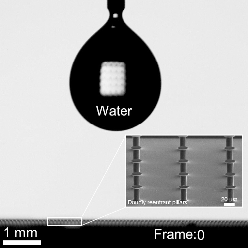
Movie S1: High speed image sequence (15K fps) of water droplet bouncing from microtextured surfaces comprising of doubly reentrant pillars. This movie was reprinted from ref 35. Copyright (2019), with permission from Elsevier. Please click here to view this video (Right click to download).
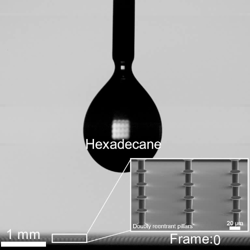
Movie S2: High speed image sequence (19K fps) of hexadecane droplet bouncing from microtextured surfaces comprising of doubly reentrant pillars. This movie was reprinted from ref 35. Copyright (2019), with permission from Elsevier. Please click here to view this video (Right click to download).
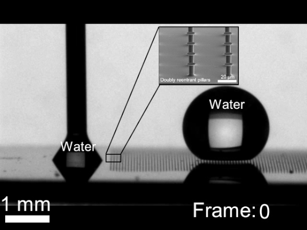
Movie S3: Image sequence (200 fps) of water imbibition into microtexture comprising of doubly reentrant pillars. This movie was reprinted from ref 35. Copyright (2019), with permission from Elsevier. Please click here to view this video (Right click to download).
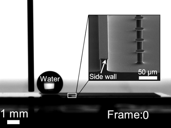
Movie S4: Image sequence (200 fps) water drop advancing next to hybrid microtexture. Presence of doubly reentrant boundary wall prevents liquid invasion into the microtexture, which makes the surface omniphobic under immersion also. This movie was reprinted from ref 35. Copyright (2019), with permission from Elsevier. Please click here to view this video (Right click to download).
Discussion
Here we discuss additional factors and design criteria to help the reader in applying these microfabrication protocols. For cavity microtextures (RCs and DRCs) the choice of pitch is crucial. Thinner walls between adjacent cavities would lead to low liquid-solid interfacial area and high liquid-vapor interfacial area, leading to high apparent contact angles34. However, thin walls could compromise the mechanical integrity of the microtexture, for instance, during handling and characterization; a little over-etching with thin walls (e.g., in step 6.6) could destroy the entire microtexture; under-etching with thin walls could also prevent the development of doubly reentrant features. If the DRC features are not fully developed, their ability to entrap air for long-term might suffer, especially if the liquid condenses inside the cavities26. For this reason, we chose the pitch in our experiments to be L = D + 12 μm (i.e., the minimum wall thickness between the cavities was 12 µm). We also fabricated doubly reentrant cavities with a smaller pitch of L = D + 5 μm, but the resulting surfaces were not homogeneous due to structural damage during microfabrication.
During the etching of the silica layer with C4F8 and O2 in step 4, the prior history of usage or the cleanliness of the reaction chamber could give variable results, despite following the same steps, for instance, in a common user facility such as in most universities. Thus, it is recommended that this step is performed in short time periods, for instance, no more than 5 min each and monitored the thickness of the silica layer by an independent technique, such as reflectometry. For our wafers with a 2.4 μm-thick silica layer, a typical etching routine took 13 min to remove silica completely from the targeted areas (Table 3). Because the photoresist was also etched during the process, this step removed 1 μm of the silica layer that was initially masked by the photoresist. Furthermore, to ensure that the etching rate was as expected, and to avoid cross-contamination from previous etch processes (a common issue in multiuser facilities), silica etching was always preceded by etching a sacrificial wafer as a precautionary step. During the development of the photoresist, the exposed surface might get contaminated with the photoresist's traces/particles, which could act as (microscopic) masks leading to the formation of pin residues. To avoid this, rigorous cleaning and storage protocols should be followed throughout the microfabrication process36.
Similarly, during the Bosch process, even though the SiO2 layer acts as a mask for the Si-layer underneath, it does get etched during long etching cycles, albeit at slower rates. Thus, the depth of the cavities or the height of the pillars is limited up to the point that the reentrant features will not be compromised. The passivation and etching times during the Bosch process should be tuned to obtain smooth walls. This can be achieved by testing recipes iteratively and observing their effects on samples, for instance, using electron microscopy.
In the case of RPs and DRPs, the longer the duration of isotropic etching, the smaller the diameter of the stem. If the diameter is less than 10 μm, it might lead to mechanical fragility. This limitation should inform the design at the beginning of the microfabrication procedure.
Dry-etching tools commonly available in universities do not have industrial-grade tolerances, leading to spatial non-uniformities in terms of the rate of etching inside the chamber. Thus, the features obtained in the center of the wafer might not be the same as those at the boundary. To overcome this limitation, we used four-inch wafers and concentrated only in the central region.
We also recommend using direct-writing systems instead of using hard-contact masks for photolithography, allowing for rapid changes in design parameters, including feature diameters, pitches and shapes (circular, hexagonal and square), etc.
Obviously, neither SiO2/Si wafers nor photolithography are the desired materials or processes for the mass production of omniphobic surfaces. However, they serve as an excellent model system to explore innovative microtextures for engineering omniphobic surfaces, for instance by biomimetics26,27,34,35,46,47, which can be translated to low-cost and scalable materials systems for applications. It is expected that in the near future, the design principles for GEMs might be scaled up using techniques such as 3-D printing48, additive manufacturing49, and laser micromachining50, among others. Microtextured SiO2/Si surfaces could also be used for templating soft materials29,51. Currently, we are investigating applications of our gas-entrapping surfaces for mitigating cavitation damage47, desalination46,52, and reducing hydrodynamic drag.
Disclosures
The authors declare that they have no competing interests.
Acknowledgements
HM acknowledges funding from King Abdullah University of Science and Technology (KAUST).
Materials
| Name | Company | Catalog Number | Comments |
| AZ-5214 E photoresist | Merck | DEAA070796-0W59 | Photoresist, flammable liquid |
| AZ-726 MIF developer | Merck | 10055824960 | To develop photoresist |
| Confocal microscopy | Zeiss | Zeiss LSM710 | Upright confocal microscope to visualize liquid meniscus shape |
| Deep ICP-RIE | Oxford Instruments | Plasmalab system100 | Silicon etching tool |
| Direct writer | Heidelberg Instruments | µPG501 | Direct-writing system |
| Drop shape analyzer | KRUSS | DSA100 | To measure contact angle |
| Hexadecane | Alfa Aesar | 544-76-3 | Test liquid |
| Highspeed imaging camera | Phantom vision research | v1212 | To image droplet bouncing |
| HMDS vapor prime | Yield Engineering systems | ||
| Hot plate | Cost effective equipments | Model 1300 | |
| Hydrogen peroxide 30% | Sigma Aldrich | 7722-84-1 | To prepare piranha solution |
| Imaris software | Bitplane | Version 8 | Post process confocal microscopy images |
| Nile Red | Sigma Aldrich | 7385-67-3 | Fluorescent dye for hexadecane |
| Nitrogen gas | KAUST lab supply | To dry the wafer | |
| Petri dish | VWR | HECH41042036 | |
| Reactive-Ion Etching (RIE) | Oxford Instruments | Plasmalab system100 | Silica etching tool |
| Reflectometer | Nanometrics | Nanospec 6100 | To check remaining oxide layer thickness |
| Rhodamine B (Acros) | Fisher scientific | 81-88-9 | Fluorescent dye for water |
| SEM stub | Electron Microscopy Sciences | 75923-19 | |
| SEM-Quanta 3D | FEI | Quanta 3D FEG Dual Beam | |
| Silicon wafer | Silicon Valley Microelectronics | Single side polished, 4" diameter, 500 µm thickness, 2.4 µm thick oxide layer | |
| Spin coater | Headway Research,Inc | PWM32 | |
| Spin rinse dryer | MicroProcess technology | Avenger Ultra -Pure 6 | Dry the wafers after piranha clean |
| Sulfuric acid 96% | Technic | 764-93-9 | To prepare piranha solution |
| Tanner EDA L-Edit software | Tanner EDA, Inc. | version15 | Layout design |
| Thermal oxide growth | Tystar furnace | To grow thermal oxide in patterned silicon wafer | |
| Tweezers | Excelta | 490-SA-PI | Wafer tweezer |
| Vacuum oven | Thermo Scientific | 13-258-13 | |
| Water | Milli-Q | Advantage A10 | Test liquid |
References
- Butt, H. J., et al. Characterization of super liquid-repellent surfaces. Current Opinion in Colloid & Interface Science. 19 (4), 343-345 (2014).
- Lee, J., Laoui, T., Karnik, R. Nanofluidic transport governed by the liquid/vapour interface. Nature Nanotechnology. 9 (4), 317-323 (2014).
- Subramanian, N., et al. Evaluating the potential of superhydrophobic nanoporous alumina membranes for direct contact membrane distillation. Journal of Colloid and Interface Science. 533, 723-732 (2019).
- Xue, Z. X., Cao, Y. Z., Liu, N., Feng, L., Jiang, L. Special wettable materials for oil/water separation. Journal of Materials Chemistry A. 2 (8), 2445-2460 (2014).
- Zhang, L. B., Zhong, Y. J., Cha, D., Wang, P. A self-cleaning underwater superoleophobic mesh for oil-water separation. Scientific Reports. 3, (2013).
- Leslie, D. C., et al. A bioinspired omniphobic surface coating on medical devices prevents thrombosis and biofouling. Nature Biotechnology. 32 (11), 1134-1140 (2014).
- Lee, C., Choi, C. H., Kim, C. J. Superhydrophobic drag reduction in laminar flows: a critical review. Experiments in Fluids. 57 (176), (2016).
- Tuteja, A., Choi, W., Mabry, J. M., McKinley, G. H., Cohen, R. E. Robust omniphobic surfaces. Proceedings of the National Academy of Sciences of the United States of America. 105 (47), 18200-18205 (2008).
- Brown, P. S., Bhushan, B. Mechanically durable, superoleophobic coatings prepared by layer-by-layer technique for anti-smudge and oil-water separation. Scientific Reports. 5, (2015).
- Wong, T. S., et al. Bioinspired self-repairing slippery surfaces with pressure-stable omniphobicity. Nature. 477 (7365), 443-447 (2011).
- Milionis, A., Dang, K., Prato, M., Loth, E., Bayer, I. Liquid repellent nanocomposites obtained from one-step water-based spray. Journal of Materials Chemistry A. 3 (24), 12880-12889 (2015).
- Mishra, H., et al. Time-Dependent Wetting Behavior of PDMS Surfaces with Bioinspired, Hierarchical Structures. ACS Applied Materials & Interfaces. 8 (12), 8168-8174 (2016).
- Hendren, Z. D., Brant, J., Wiesner, M. R. Surface modification of nanostructured ceramic membranes for direct contact membrane distillation. Journal of Membrane Science. 331 (12), 1-10 (2009).
- Rezaei, M., et al. Wetting phenomena in membrane distillation: Mechanisms, reversal, and prevention. Water Research. 139, 329-352 (2018).
- Verho, T., et al. Mechanically Durable Superhydrophobic Surfaces. Advanced Materials. 23, 673-678 (2011).
- Boinovich, L., Emelyanenko, A. M., Pashinin, A. S. Analysis of Long-Term Durability of Superhydrophobic Properties under Continuous Contact with Water. ACS Applied Materials & Interfaces. 2 (6), 1754-1758 (2010).
- Herminghaus, S. Roughness-induced non-wetting. Europhysics Letters. 52 (2), 165-170 (2000).
- Abdelsalam, M. E., Bartlett, P. N., Kelf, T., Baumberg, J. Wetting of regularly structured gold surfaces. Langmuir. 21 (5), 1753-1757 (2005).
- Liu, J. L., Feng, X. Q., Wang, G. F., Yu, S. W. Mechanisms of superhydrophobicity on hydrophilic substrates. Journal of Physics-Condensed Matter. 19 (35), (2007).
- Nosonovsky, M. Multiscale roughness and stability of superhydrophobic biomimetic interfaces. Langmuir. 23 (6), 3157-3161 (2007).
- Marmur, A. From hygrophilic to superhygrophobic: Theoretical conditions for making high-contact-angle surfaces from low-contact-angle materials. Langmuir. 24 (14), 7573-7579 (2008).
- Hensel, R., et al. Wetting Resistance at Its Topographical Limit: The Benefit of Mushroom and Serif T Structures. Langmuir. 29 (4), 1100-1112 (2013).
- Bormashenko, E. Progress in understanding wetting transitions on rough surfaces. Advances in Colloid and Interface Science. 222, 92-103 (2015).
- Patankar, N. A. Thermodynamics of trapping gases for underwater superhydrophobicity. Langmuir. 32 (27), 7023-7028 (2016).
- Kaufman, Y., et al. Simple-to-Apply Wetting Model to Predict Thermodynamically Stable and Metastable Contact Angles on Textured/Rough/Patterned Surfaces. The Journal of Physical Chemistry C. 121 (10), 5642-5656 (2017).
- Domingues, E. M., Arunachalam, S., Nauruzbayeva, J., Mishra, H. Biomimetic coating-free surfaces for long-term entrapment of air under wetting liquids. Nature Communications. 9 (1), 3606(2018).
- Liu, T. Y., Kim, C. J. Turning a surface superrepellent even to completely wetting liquids. Science. 346 (6213), 1096-1100 (2014).
- Hensel, R., Neinhuis, C., Werner, C. The springtail cuticle as a blueprint for omniphobic surfaces. Chemical Society Reviews. 45 (2), 323-341 (2016).
- Hensel, R., et al. Biologically Inspired Omniphobic Surfaces by Reverse Imprint Lithography. Advanced Materials. 26 (13), 2029-2033 (2014).
- Hensel, R., et al. Tunable nano-replication to explore the omniphobic characteristics of springtail skin. Npg Asia Materials. 5, (2013).
- Helbig, R., Nickerl, J., Neinhuis, C., Werner, C. Smart Skin Patterns Protect Springtails. PLOS ONE. 6 (9), 25105(2011).
- Cheng, L. Marine and Freshwater Skaters: Differences in Surface Fine Structures. Nature. 242, 132(1973).
- Andersen, N. M., Cheng, L. The marine insect Halobates (Heteroptera: Gerridae): biology, adaptations, distribution, and phylogeny. Oceanography and marine biology: an annual review. 42, 119-180 (2004).
- Domingues, E. M., Arunachalam, S., Mishra, H. Doubly Reentrant Cavities Prevent Catastrophic Wetting Transitions on Intrinsically Wetting Surfaces. ACS Applied Materials & Interfaces. 9 (25), 21532-21538 (2017).
- Arunachalam, S., Das, R., Nauruzbayeva, J., Domingues, E. M., Mishra, H. Assessing omniphobicity by immersion. Journal of Colloid and Interface Science. 534, 156-162 (2019).
- Christian Koch, E. A. Photolithography: Basics of Microstructuring. , MicroChemicals GmbH. (2017).
- Jansen, H., de Boer, M., Legtenberg, R., Elwenspoek, M. The black silicon method: a universal method for determining the parameter setting of a fluorine-based reactive ion etcher in deep silicon trench etching with profile control. Journal of Micromechanics and Microengineering. 5 (2), 115(1995).
- Jansen, H. V., de Boer, M. J., Unnikrishnan, S., Louwerse, M., Elwenspoek, M. C. Black silicon method X: a review on high speed and selective plasma etching of silicon with profile control: an in-depth comparison between Bosch and cryostat DRIE processes as a roadmap to next generation equipment. Journal of Micromechanics and Microengineering. 19 (3), 033001(2009).
- Xiu, Y., Zhu, L., Hess, D. W., Wong, C. Hierarchical silicon etched structures for controlled hydrophobicity/superhydrophobicity. Nano Letters. 7 (11), 3388-3393 (2007).
- Azeredo, B., et al. Silicon nanowires with controlled sidewall profile and roughness fabricated by thin-film dewetting and metal-assisted chemical etching. Nanotechnology. 24 (22), 225305(2013).
- Coffinier, Y., et al. Preparation of superhydrophobic silicon oxide nanowire surfaces. Langmuir. 23 (4), 1608-1611 (2007).
- Tanner, E. L-Edit-The layout editor. Reference Manual. , Available from: https://usermanual.wiki/Document/LEdit20Manual.38314693/view (2009).
- NANOSPEC 6100 Series Operators Users Manual. , Nanometrics. Available from: https://cmi.epfl.ch/metrology/Nanospec_AFT6100_Manual.pdf (2019).
- Deal, B. E., Grove, A. General relationship for the thermal oxidation of silicon. Journal of Applied Physics. 36 (12), 3770-3778 (1965).
- Woollam, J. A., et al. Spectroscopic ellipsometry from the vacuum ultraviolet to the far infrared. AIP Conference Proceedings. 550 (1), 511-518 (2001).
- Das, R., Arunachalam, S., Ahmad, Z., Manalastas, E., Mishra, H. Bio-inspired gas-entrapping membranes (GEMs) derived from common water-wet materials for green desalination. Journal of Membrane Science. , 117185(2019).
- Gonzalez-Avila, S. R., Nguyen, D. M., Arunachalam, S., Domingues, E. M., Mishra, H., Ohl, C. D. Mitigating cavitation erosion using biomimetic gas-entrapping microtextured surfaces. Science Advances. , In-press (2020).
- Liu, X., et al. 3D Printing of Bioinspired Liquid Superrepellent Structures. Advanced Materials. 30 (22), 1800103(2019).
- Jafari, R., Cloutier, C., Allahdini, A., Momen, G. Recent progress and challenges with 3D printing of patterned hydrophobic and superhydrophobic surfaces. The International Journal of Advanced Manufacturing Technology. , 1-14 (2019).
- Vorobyev, A. Y., Guo, C. L. Multifunctional surfaces produced by femtosecond laser pulses. Journal of Applied Physics. 117 (3), 033103(2015).
- Xu, M., Kim, C. J. Method for manufacturing re-entrant microstructures. US Patent App. , 15/546,260 (2018).
- Das, R., Arunachalam, S., Ahmad, Z., Manalastas, E., Syed, A., Buttner, U., Mishra, H. Proof-of-Concept for Gas-Entrapping Membranes Derived from Water-Loving SiO2/Si/SiO2 Wafers for Greener Desalination. Journal of Visualized Experiments. , In-press e60583(2020).
Reprints and Permissions
Request permission to reuse the text or figures of this JoVE article
Request PermissionThis article has been published
Video Coming Soon
Copyright © 2025 MyJoVE Corporation. All rights reserved