
A subscription to JoVE is required to view this content. Sign in or start your free trial.
Method Article
Rapid Fabrication of Custom Microfluidic Devices for Research and Educational Applications
In This Article
Summary
Here we present a protocol to design and fabricate custom microfluidic devices with minimal financial and time investment. The aim is to facilitate the adoption of microfluidic technologies in biomedical research laboratories and educational settings.
Abstract
Microfluidic devices allow for the manipulation of fluids, particles, cells, micro-sized organs or organisms in channels ranging from the nano to submillimeter scales. A rapid increase in the use of this technology in the biological sciences has prompted a need for methods that are accessible to a wide range of research groups. Current fabrication standards, such as PDMS bonding, require expensive and time consuming lithographic and bonding techniques. A viable alternative is the use of equipment and materials that are easily affordable, require minimal expertise and allow for the rapid iteration of designs. In this work we describe a protocol for designing and producing PET-laminates (PETLs), microfluidic devices that are inexpensive, easy to fabricate, and consume significantly less time to generate than other approaches to microfluidics technology. They consist of thermally bonded film sheets, in which channels and other features are defined using a craft cutter. PETLs solve field-specific technical challenges while dramatically reducing obstacles to adoption. This approach facilitates the accessibility of microfluidics devices in both research and educational settings, providing a reliable platform for new methods of inquiry.
Introduction
Microfluidics enables fluid control at small scales, with volumes ranging from microliters (1 x 10⁻⁶ L) to picoliters (1 x 10-12 L). This control has been made possible in part due to the application of microfabrication techniques borrowed from the microprocessor industry1. The use of micro-sized networks of channels and chambers allows the user to take advantage of the distinct physical phenomena characteristic of small dimensions. For example, at the micrometer scale, fluids can be manipulated using laminar flow, where viscous forces dominate inertial forces. As a result, diffusive transport becomes the prominent feature of microfluidics, and can be studied quantitatively and experimentally. These systems can be properly understood using Fick’s laws, Brownian motion theory, the heat equation, and/or the Navier-Stokes equations, which are important derivations in the fields of fluid mechanics and transport phenomena2.
Because many groups in the biological sciences study complex systems at the microscopic level, it was originally thought that microfluidic devices would have an immediate and significant impact on research applications in biology2,3. This is due to diffusion being dominant in the transport of small molecules across membranes or within a cell, and the dimensions of cells and microorganisms are an ideal match for sub-millimeter systems and devices. Therefore, there was significant potential for enhancing the way in which cellular and molecular experimentation is conducted. However, wide adoption of microfluidic technologies by biologists has lagged behind expectations4. A simple reason for the lack of technology transfer may be the disciplinary boundaries separating engineers and biologists. Custom device design and fabrication have remained just outside of the capabilities of most biological research groups, making them dependent on external expertise and facilities. Lack of familiarity with potential applications, cost, and the time required for design-iteration are also significant barriers for new adopters. It is likely that these barriers have had the effect of disrupting innovation and preventing the widespread application of microfluidics to address challenges in the biological sciences.
A case in point: Since the late 1990’s soft-photolithography has been the method of choice for the fabrication of microfluidic devices. PDMS (polydimethylsiloxane, a silicone-based organic polymer) is a widely used material because of its physical properties, such as transparency, deformability, and biocompatibility5. The technique has enjoyed great success, with lab-on-a-chip and organ-on-a-chip devices continually being developed on this platform6. Most of the groups working on these technologies, however, are found in engineering departments or have strong ties to them4. Lithography usually requires clean-rooms for the fabrication of molds and specialized bonding equipment. For many groups, this makes standard PDMS devices less than ideal due their capital costs and lead-time, particularly when there is a need to make repeated design modifications. Furthermore, the technology is mostly inaccessible to the average biologist and to students without access to specialized engineering laboratories. It has been proposed that for microfluidic devices to be widely adopted, they must mimic some of the qualities of materials commonly used by biologists. For example, polystyrene used for cell culture and bioassays is inexpensive, disposable, and amenable to mass production. In contrast, industrial manufacturing of PDMS-based microfluidics has never been realized because of its mechanical softness, surface treatment instability, and gas permeability5. Because of these limitations, and with the goal of solving technical challenges using customized devices built “in-house”, we describe an alternative method that utilizes xurography7,8,9 protocols and thermal lamination. This method can be adopted with little capital and time investment.
PETLs are fabricated using polyethylene terephthalate (PET) film, coated with the thermoadhesive ethylene-vinyl acetate (EVA). Both materials are widely used in consumer products, are biocompatible and are readily available at minimal cost10. PET/EVA film can be obtained in the form of laminating pouches or rolls. Using a computer-controlled craft cutter commonly found in hobbyist or craft stores, channels are cut out of a single film sheet to define the device’s architecture11. The channels are then sealed by applying additional film (or glass) layers that are bonded using an (office) thermal laminator (Figure 1A). Perforated, self-adhesive vinyl bumpers are added to facilitate access to the channels. Fabrication times range from 5 to 15 min, which allows rapid design iteration. All the equipment and materials used to make PETLs are commercially accessible and affordable (<350 USD starting cost, compared to thousands of USDs for lithography). Therefore, PETLs provide a novel solution to two main problems posed by conventional microfluidics: affordability and time effectiveness (See PDMS/PETL comparison in Supplementary Tables 1, 2).
In addition to providing researchers with the opportunity to design and fabricate their own devices, PETLs can be easily adopted in the classroom because they are simple and intuitive to use. PETLs can be included in high school and college curricula8, where they are used to help students better understand physical, chemical and biological concepts, like diffusion, laminar flow, micromixing, nanoparticle synthesis, gradient formation and chemotaxis.
In this work we illustrate the overall workflow for the fabrication of model PETLs chips with different levels of complexity. The first device is used to facilitate imaging of cells and micro-organs in a small chamber. The second, more complex device consists of several layers and materials, and is used for research in mechanobiology9. Lastly, we built a device that displays several fluid dynamics concepts (hydrodynamic focusing, laminar flow, diffusive transport and micromixing) for educational purposes. The workflow and device designs presented here can be easily tailored for a large range of purposes in both the research and classroom settings.
Access restricted. Please log in or start a trial to view this content.
Protocol
1. Design
- Identify an application for the devices and list the channel/chamber components that will be required.
NOTE: All devices will require input and output channels. Devices used for microscopy will require an imaging chamber. More complex devices will require channels and chambers situated in multiple layers. - Start by hand-drawing each layer, considering how the device’s functionality is affected by the superposition of the layers.
- Draw the final designs on a computer using any software that allows for drawing lines and shapes.
- Draw each layer separately using black, solid lines and shapes devoid of shades. Line thickness of 6 or more points are recommended. At this stage, the dimensions of channel and chamber features are less important than the overall proportions.
- Use the copy-and-paste function when creating features and superimposing layers. See Figure 1B for examples of layer drawings.
- Import each layer into the craft cutter software (Figure 1C). Do this by making a screen capture of the drawn design and using a drag and drop approach.
- Create a new document in the craft cutter software (free download). Drop the image file on the mat displayed. The software will recognize most image files.
- Enlarge the image to facilitate processing by pulling from a corner. The design can now be recognized by the software using the trace function.
NOTE: Users may produce de novo designs directly on this software (use drawing tools in design palette).
- To trace the design, select the Trace icon (shape of a butterfly) on the right side of the window and completely select the imported designs.
- Select the Trace Preview option labeled outline. Adjust (if needed) the Threshold and Scale settings to adjust the yellow trace to match the design.
- Select Trace from the Trace menu once the yellow trace matches the design. The channels are now shown as a red contour. If the red contour matches the design, the imported image can be selected and deleted. The design is now imported and ready for sizing.
- Size the device by selecting the traced design and by using the grid provided by the software. Pull to change the width and length of channels and chambers.
NOTE: The software provides measurements, and small lines can be drawn temporarily (use design palette on the left side of the window) to measure dimensions within the device. Functional channel-width dimensions range from 100 µm to 900 µm. Dimensions may have to be adjusted after testing initial prototypes. It is important that all layers are sized proportionally, to ensure proper alignment during assembly.- After the design is properly sized, select the square tool on the shape drawing menu to draw a square/rectangle around each layer of the device. This shape should be of the same size for all layers. See Figure 1C for examples.
- Create a separate top layer containing access ports to the channels. Simple designs will consist of a main (middle) channel layer, a bottom sealing layer (often glass) and a top layer that should contain circular perforations to access the channels (inlets/outlets).
NOTE: Designs containing more than three layers will require inlet/outlet perforations in multiple layers (See Figure 1C, Figure 5A). These perforations may be already included in the design, or can be added at this time.- Select the drawing tool on the left side of the screen. Draw circles over the inlet and outlet ports of the design.
- Copy and paste both the original design and the circles. Erase the channels from the underlying device.
NOTE: This leaves the inlet/outlet ports in the right position corresponding to the original design. Shapes may also be added to the periphery of each layer to aid with aligning.
- Arrange all layers to be cut on the displayed mat. The device is now ready for cutting.
2. Cutting
- Apply a single PET/EVA film (or other material) of preferred thickness (3 mil is standard) onto the adhesive cutting mat. Make sure the adhesive (matte) side faces up and the plastic (shiny) side faces down.
NOTE: Use clean gloves to avoid introducing oils and microparticles to the layers. - Flatten the film against the mat (Figure 1D), removing all air that may have been trapped. This can be done using gloved hands or a roller.
- Align the edge of the cutting mat to the line indicated on the cutter. Load the mat by pressing Load Mat on the cutter. Keep the setting on the cutting blade between 3 and 5, depending on the film thickness.
- Connect the cutter USB cable to the computer.
- Select the SEND tab and select a cutting setting.
NOTE: A multitude of settings are available on the cascade menu. The -Sticker Paper, Clear- is a setting that works well with PET/EVA film that has a thickness of 3–5 mil (75–125 μm). Modify settings for different materials and save custom settings for future use.
- Select the SEND tab and select a cutting setting.
- Click Send. Cutting will begin (Figure 1E). Make sure there is enough room in the back of the cutter for the mat to move unimpeded. When the cutter is finished, unload the mat by selecting Unload on the cutter. Do not pull the mat out before unloading.
3. Alignment
- Place the cutting mat next to a clean surface. With gloved hands, use a pair of tweezers to lift each layer of the microfluidics device off the cut mat (Figure 1F). Be especially careful around turns and bends in the channel; these are especially delicate and susceptible to tearing and warping.
- Place the layers of the microfluidics device onto a clean surface. Order them according to their top-to-bottom position in the device (Figure 1G, Figure 2A, Figure 5A and Figure 7A).
- Cut small (~3 mm x 10 mm) pieces of double-sided tape that will be used to temporarily attach the layers together.
- Superimpose the layers one by one, starting with the bottom layer. Add a small piece of double-sided tape to a corner between the layers, away from any channels or inlets/outlets (Figure 1G, arrow). The tape, although not required, immobilizes the layers and assures they will not shift during lamination. Use a wire jig to facilitate the alignment of layers in devices with more than 4 layers (Supplementary Figure 3).
- Ensure that the adhesive (matte-EVA) side of the film always faces the inside (within-layers portion) of the device.
CAUTION: Exposed adhesive will melt against the internal parts of the laminator and adhere to them, resulting not only in the loss of the device but also affecting the future performance of the laminator. - Once all layers have been superimposed, inspect the device. There should be at least one EVA side in between all layers, and no EVA should be exposed. When introducing non-EVA coated materials (e.g., polyvinyl chloride (PVC) film, glass), a film coated with EVA on both sides might be needed, particularly in the case of more complex devices (Figure 5).
4. Lamination
- Turn on and set the laminator to the desired thickness setting. Some laminators offer 3 and 5 mil settings, while some do not. For any device with 4 or more layers, use the 5-mil setting.
- Once the laminator is ready, run the device through the laminating rollers (Figure 1H–I). Place the end to which double sided tape has been added for best results.
NOTE: When fabricating devices of five or more layers, they may be run through the laminator more than once. - Recover the laminated device.
NOTE: It is advisable for devices to be large enough as to make easy their recovery from the laminator. This consideration does not affect the size of the channels or chip architecture, it simply calls for a “frame” that can easily go through the laminator without remaining inside.
5. Inlet/outlet ports
- Use a rotary tool and a 1/32 in. drill bit to cut a small hole through the center of a furniture bumper. Alternatively, use a 1 mm biopsy punch to perforate the bumpers.
NOTE: A drill press is recommended. Although sizes vary, 2 mm x 6 mm-diameter bumpers are recommended. Avoid simply “stabbing” the bumper. Unless material is removed, the bumper will seal again (Supplementary Figure 1). The perforations as indicated above are meant to interface with polyetheretherketone (PEEK) tubing, a pipette and tip, or a blunt needle (16–18 G). Larger perforations can be achieved using revolving punch pliers (Supplementary Figure 1). These are useful when the bumper is used as a “reservoir” for liquids or other biologicals. - Make sure that the orifice is completely clear by removing any debris (caused by drilling or punching) with a pair of small tweezers.
- After the inlet/outlet ports are successfully cleared, carefully align the bumpers with the inlet/outlet ports on the laminated device (Figure 1J–K). This step is essential to having proper flow of liquids in and out of the device. Hold the bumper behind the device, position the adhesive face facing the open inlet/outlet on the device, then align and adhere. Device assembly is now completed.
6. Testing
- Access the channel/chamber architectures through the perforated bumpers (ports). There are several options regarding how to introduce fluids and biologicals into the devices.
- Use laboratory or medical/surgical tubing by attaching it to a plastic connector (e.g., Luer adaptors) or to a blunt needle. A standard pipette and tip or PEEK tubing without adaptors can also be used (Supplementary Figure 2).
- Perform infusion or drawing of fluids with syringes and tubing using syringes or peristaltic pumps.
NOTE: There are many options in the market, starting at ~300 USD at the time of writing. - Set different flow rate settings according to the device and experiment.
NOTE: We routinely use flow rate settings in the range of 0.01–100 µL/min, but other rates can be used.

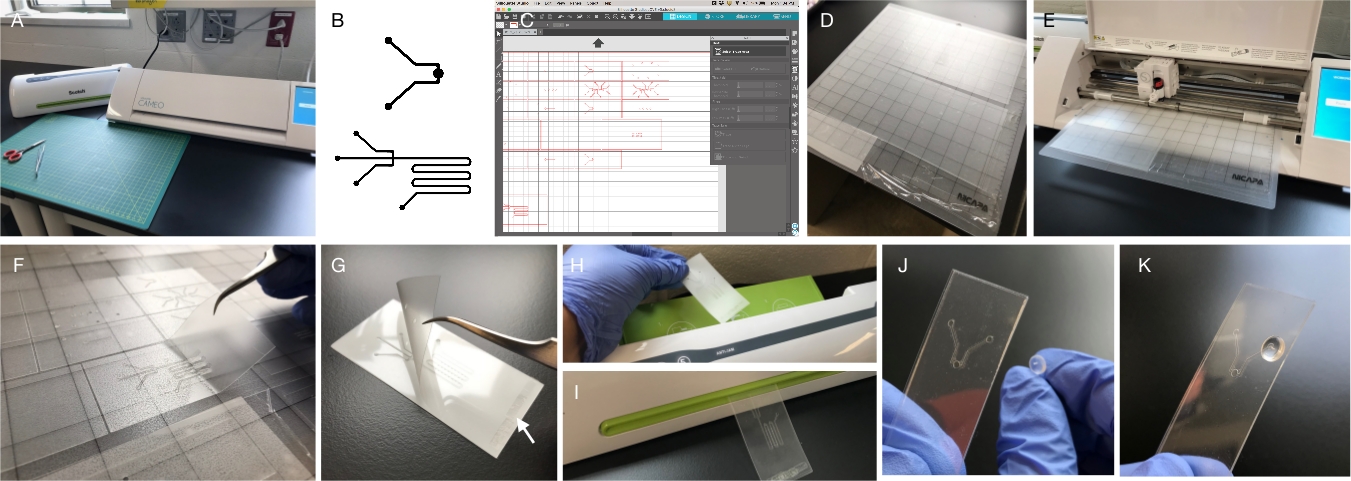
Figure 1: Fabrication. (A) An office laminator and a craft cutter are the only two pieces of equipment required for fabrication. Both are available online or at crafts/office supplies stores. Other required tools include scissors and tweezers. (B) Channel and chamber architectures can be composed digitally using any software program that includes drawing tools (vector graphics may be preferred by some users, but are not required). Lines and shapes are drawn in black with a white background. The file or a screen capture of the design can be imported into the craft cutter software by dragging and dropping. (C) Craft cutter software is available free to download and is required to control the cutter. The software acquires the design and allows for modifications, like sizing. It also provides drawing tools. (D) The cutting mat carries the film for cutting. It is slightly adhesive, allowing for immobilization of the materials to be cut. The figure shows four different materials ready for loading: 3 mil-thick PET/EVA film (top), 5 mil-thick PET/EVA film (middle), 6 mil-thick EVA/PET/EVA (bottom left) and PVC film (bottom right). (E) Cutter is open to display blade (in black) unit and loaded mat. (F) After cutting, individual layers are lifted using tweezers. Cut outs of channels and chambers remain attached to the mat and are later removed and discarded. (G) Individual layers are aligned and superimposed for lamination. Small pieces of double-sided tape (arrow) are often used to aid in aligning and prevent layer shifting during lamination. (H, I) The device is fed at the top of the laminator and recovered through the slot. Lamination provides a robust seal, leaving channel paths open. (J, K) In order to access the channels, it is necessary to add perforated, self-adhesive vinyl bumpers. Image in (J) displays the “reverse” approach for alignment, in which the bumper is placed from the back, allowing visual alignment of the inlet/outlet with the bumper perforation. Please click here to view a larger version of this figure.
Access restricted. Please log in or start a trial to view this content.
Results
In addition to low cost and rapid iteration, PETL technology can be easily customized to solve specific challenges. First, we describe a simple device consisting of a glass coverslip, a chamber layer, a channel layer, and an inlet/outlet layer (Figure 2). This device was designed to facilitate the imaging of cells and micro-organs under constant flow. Culture medium is replenished at low flow rates to encourage nutrient and gas exchange. The round chamber features a glass bottom, which allow...
Access restricted. Please log in or start a trial to view this content.
Discussion
While microfluidics are increasingly present in the toolbox of laboratories around the world, the pace of adoption has been disappointing, given the potential for its positive impact16. Low cost and high efficiency of microfluidic device fabrication are essential to accelerate adoption of this technology in the average research laboratory. The method described here uses multiple film layers to create two and three-dimensional devices at a fraction of the time and cost required by lithographic meth...
Access restricted. Please log in or start a trial to view this content.
Disclosures
Fernando Ontiveros is in the process of launching PETL FLUIDICS (LLC), a company that will commercialize and provide consulting services for this technology. The co-authors have nothing to disclose.
Acknowledgements
The work in this manuscript was supported in part by the National Science Foundation (NSF) (Grant No. CBET-1553826) (and associated ROA supplement) and the National Institutes of Health (NIH) (Grant No. R35GM124935) to J.Z., and the Notre Dame Melchor Visiting Faculty fund to F.O. We would like to thank Jenna Sjoerdsma and Basar Bilgiçer for providing mammalian cells and culture protocols and Fabio Sacco for assistance with supplementary figures.
Access restricted. Please log in or start a trial to view this content.
Materials
| Name | Company | Catalog Number | Comments |
| Biopsy punch (1mm) | Miltex | 33-31AA | Optional, replaces rotary tool set up |
| Blunt needles | Janel, Inc. | JEN JG18-0.5X-90 | Remove plastic and attach to Tygon tubing |
| Coverslips | Any | 24 x 60 mm are preferred | |
| Cutting Mat and blades | Silhouette America or Nicapa | www.silhouetteamerica.com/shop/blades-and-mats | Re-use/Disposables |
| Double-sided tape | Scotch/3M | 667 | Small amounts, any width or brand |
| PEEK tubing | IDEX/any | 1581L | Different configurations available. Consider using Tygon tubing intead, if not already using PEEK |
| PET/EVA thermal laminate film | Scotch/3M & Transcendia | TP3854-200,TP5854-100 & transcendia.com/products/trans-kote-pet | 3 - 6 mil (mil = 1/1000 inch) laminating pouches or rolls. |
| PVC film - Cling Wrap | Glad / Any | Food wrapping | |
| Rotary tool-drill | Dremel/Any | 200-121 or other | 1/32 and 3/64" drill bits from Dremel recommended |
| Rubber Roller | Speedball | 4126 | To facilitate adhesion, any brand will work |
| Scissors & tweezers | Any | Fiskars-Inch-Titanium-Softgrip-Scissors |Cole-Parmer –# UX-07387-12 | Quality brands are recommended |
| Silhouette CAMEO Craft cutter | Silhouette America | www.silhouetteamerica.com/shop/cameo/SILHOUETTE-CAMEO-3-4T | Preferred craft cutter |
| Silhouette Studio software | Silhouette America | www.silhouetteamerica.com/software | Controls the craft cutter and provides drawing tools (free download MAC and PC) |
| Syringe Pump | Harvard Apparatus or New Era | 70-4504 or NE-300 | Pumps are ideal, pipettes or burettes can be used. |
| Syringes | Any | 1-3mL | |
| Thermal laminator | Scotch/3M | TL906 | Standard home/office model |
| Tygon tubing (E-3603) | Cole-Parmer | EW-06407-70 | Use with blunt needle tips |
| Vinyl furniture bumpers | DerBlue/3M/ Everbilt | Clear, self-adhesive (6 x 2 mm and 8 x 3 mm) | Round bumpers are recommended |
References
- Xia, Y., Whitesides, G. M. SOFT LITHOGRAPHY. Annual Review of Materials Science. 28 (1), 153-184 (1998).
- Beebe, D. J., Mensing, G. A., Walker, G. M. Physics and Applications of Microfluidics in Biology. Annual Review of Biomedical Engineering. 4 (1), 261-286 (2002).
- Whitesides, G. M., Ostuni, E., Takayama, S., Jiang, X., Ingber, D. E. Soft Lithography in Biology and Biochemistry. Annual Review of Biomedical Engineering. 3 (1), 335-373 (2001).
- Sackmann, E. K., Fulton, A. L., Beebe, D. J. The present and future role of microfluidics in biomedical research. Nature. 507 (7491), 181-189 (2014).
- Berthier, E., Young, E. W. K., Beebe, D. Engineers are from PDMS-land, Biologists are from Polystyrenia. Lab on a Chip. 12 (7), 1224(2012).
- Zhang, B., Korolj, A., Lai, B. F. L., Radisic, M. Advances in organ-on-a-chip engineering. Nature Reviews Materials. 3 (8), 257-278 (2018).
- Bartholomeusz, D. A., Boutte, R. W., Andrade, J. D. Xurography: rapid prototyping of microstructures using a cutting plotter. Journal of Microelectromechanical Systems. 14 (6), 1364-1374 (2005).
- Martínez-Hernández, K. J., Rovira-Figueroa, N. D., Ontiveros, F. Implementation and Assessment of Student-Made Microfluidic Devices in the General Chemistry Laboratory. , (2016).
- Levis, M., et al. Microfluidics on the fly: Inexpensive rapid fabrication of thermally laminated microfluidic devices for live imaging and multimodal perturbations of multicellular systems. Biomicrofluidics. 13 (2), 024111(2019).
- Subramaniam, A., Sethuraman, S. Chapter 18 - Biomedical Applications of Nondegradable Polymers. Natural and Synthetic Biomedical Polymers. , 301-308 (2014).
- Yuen, P. K., Goral, V. N. Low-cost rapid prototyping of flexible microfluidic devices using a desktop digital craft cutter. Lab Chip. 10 (3), 384-387 (2010).
- Oya, K., et al. Surface Characteristics of Polyethylene Terephthalate (PET) Film Exposed to Active Oxygen Species Generated via Ultraviolet (UV) Lights Irradiation in High and Low Humidity Conditions. Journal of Photopolymer Science and Technology. 27 (3), 409-414 (2014).
- Narciso, C. E., Contento, N. M., Storey, T. J., Hoelzle, D. J., Zartman, J. J. Release of Applied Mechanical Loading Stimulates Intercellular Calcium Waves in Drosophila Wing Discs. Biophysical Journal. 113 (2), 491-501 (2017).
- Suh, Y. K., Kang, S. A Review on Mixing in Microfluidics. Micromachines. 1 (3), 82-111 (2010).
- Jahn, A., Vreeland, W. N., Gaitan, M., Locascio, L. E. Controlled Vesicle Self-Assembly in Microfluidic Channels with Hydrodynamic Focusing. Journal of the American Chemical Society. 126 (9), 2674-2675 (2004).
- Weibel, D., Whitesides, G. Applications of microfluidics in chemical biology. Current Opinion in Chemical Biology. 10 (6), 584-591 (2006).
- Chen, X., Li, T., Shen, J. CO2 Laser Ablation of Microchannel on PMMA Substrate for Effective Fabrication of Microfluidic Chips. International Polymer Processing. 31 (2), 233-238 (2016).
- Chen, X., Shen, J., Zhou, M. Rapid fabrication of a four-layer PMMA-based microfluidic chip using CO2-laser micromachining and thermal bonding. Journal of Micromechanics and Microengineering. 26 (10), 107001(2016).
Access restricted. Please log in or start a trial to view this content.
Reprints and Permissions
Request permission to reuse the text or figures of this JoVE article
Request PermissionThis article has been published
Video Coming Soon
Copyright © 2025 MyJoVE Corporation. All rights reserved