Method Article
3D Depth Profile Reconstruction of Segregated Impurities Using Secondary Ion Mass Spectrometry
In This Article
Summary
The presented method describes how to identify and solve measurement artifacts related to secondary ion mass spectrometry as well as obtain realistic 3D distributions of impurities/dopants in solid state materials.
Abstract
The presented protocol combines excellent detection limits (1 ppm to 1 ppb) using secondary ion mass spectrometry (SIMS) with reasonable spatial resolution (~1 µm). Furthermore, it describes how to obtain realistic three-dimensional (3D) distributions of segregated impurities/dopants in solid state materials. Direct 3D depth profile reconstruction is often difficult to achieve due to SIMS-related measurement artifacts. Presented here is a method to identify and solve this challenge. Three major issues are discussed, including the i) nonuniformity of the detector being compensated by flat-field correction; ii) vacuum background contribution (parasitic oxygen counts from residual gases present in the analysis chamber) being estimated and subtracted; and iii) performance of all steps within a stable timespan of the primary ion source. Wet chemical etching is used to reveal the position and types of dislocation in a material, then the SIMS result is superimposed on images obtained via scanning electron microscopy (SEM). Thus, the position of agglomerated impurities can be related to the position of certain defects. The method is fast and does not require sophisticated sample preparation stage; however, it requires a high-quality, stable ion source, and the entire measurement must be performed quickly to avoid deterioration of the primary beam parameters.
Introduction
Secondary ion mass spectrometry (SIMS) is a well-known technique used for contamination monitoring with excellent detection limits1,2,3,4,5,6. Vacuum background contribution can be problematic for light elements (e.g., hydrogen, carbon, nitrogen, oxygen), which may be present in the form of residual gases in a measurement chamber. Peres et al. previously established a technique to estimate background contribution; thus, a realistic concentration of contaminating atoms can be determined7.
In many materials, the distribution of contaminating atoms is not uniform. The case of gallium nitride (GaN) is particularly interesting, as it is predicted that oxygen mainly decorates screw and mixed dislocations8,9,10,11. Considering that most analytical methods lack sensitivity or spatial resolution to detect low concentration contaminating atoms, it is essential to develop a SIMS measurement procedure that is capable of 3D localization of segregated impurities12.
While many SIMS spectrometers are equipped with position sensitive detectors, a direct three-dimensional (3D) reconstruction of a depth profile is insufficient to obtain realistic distribution of oxygen atoms in a GaN sample. Imperfection of the detector may distort the image and prevent researchers from obtaining a realistic distribution of contaminating atoms. However, a large problem is vacuum background contribution, as usually >90% of registered oxygen counts originate from residual gases present in the analysis chamber. Presented here is a method to identify and adequately solve each of these challenges.
Nonuniformity of the detector can be tested on a blank silicon wafer. Even a long integration time can lead to the observation of some secondary ion image nonuniformity, due to varying sensitivity of each channel in a microchannel plate detector. Therefore, flat-field correction is needed to obtain high-quality images of 3D distributions of segregated atoms.
Vacuum background contribution is related to a flux of contaminating atoms from the vacuum adsorbed onto the analyzing area. Considering that the process is dynamic (i.e., the sample surface is constantly sputtered by the primary beam), it can be assumed that each point of the analyzed area has the same probability to adsorb these oxygen atoms. Furthermore, they are almost immediately sputtered and do not have enough time to segregate. Therefore, a statistical approach is the most efficient. Random elimination of 90% (or more) of oxygen counts should reveal regions where oxygen is agglomerated.
It should be noted that the stability of the primary beam is crucial for this type of experiment. After some time, the intensity and homogeneity of the beam deteriorates, which reduces the quality of the image. It is therefore essential to estimate a timespan of stable operation of the beam and perform all experiments before the beam becomes unstable. The protocol can be easily used for other materials and detected elements at which nonuniform distribution is expected. It is particularly interesting to combine this with wet chemical etching, which reveals the positions and types of dislocation. Thus, the position of agglomerated impurities can be correlated to the position of defects.
Protocol
1. Defect selective etching
- Solid etchant preparation
- Prepare eutectic mixture of strong bases of potassium hydroxide (KOH) and sodium hydroxide (NaOH), together with magnesium oxide (MgO), by dissolving and mixing the composing alkali hydroxides and metal oxide in distilled water. Keep stoichiometric quantities of 53.6/37.3/9.1 at % of NaOH, KOH, and MgO, respectively13. MgO addition increases the etchant viscosity such that it remains on the Ga-polar surface and does not flow over the edges to the N-polar surface13,14. All chemicals used should be practical grade quality.
- Heat the mixture in a flask on a hot plate to 200 °C and agitate by magnetic stirring for 1 h (above the melting point of the KOH-NaOH eutectic point).
- Cool the mixture to ~100 °C by reducing the temperature of a hot plate to completely evaporate the remaining liquid. This step depends on flask size and water volume, so it may require several minutes up to 1 h.
- Transfer the solid etchant (denoted as E+M) into a dried bottle, avoiding exposure to moisture.
CAUTION: KOH and NaOH may cause skin irritation and eye damage. Work with gloves and goggles. The protocol can also be paused here.
- Defect selective etching
- Prepare a clean GaN surface for the analysis. GaN that is epitaxially grown on sapphire is used in the following steps12.
- Place the GaN sample on a hot plate heated to ~450 °C. Place the thermocouple near the sample to precisely read the real temperature.
- Place a piece of solid E+M etchant on top of the GaN and leave for 3 min.
- Take the sample from the hot plate and place in a beaker with hot HCl for 3-5 min to eliminate remaining E+M.
- Remove the sample from HCl and insert in a beaker with deionized (DI) water and ultrasonic bath for 5-10 min.
- Dry the sample by N2 blowing.
CAUTION: HCl may cause skin irritation and eye damage. Work with gloves and goggles. Avoid getting burnt. The protocol can also be paused here.
2. Scanning electron microscopy (SEM) observation
- Mark the sample (e.g., with an L-shaped scratch using a diamond pen cutter).
- Mount the sample on a metal stub dedicated to the SEM model to be used, using a conductive adhesive (i.e., double-sided carbon conductive tape or a similar material). Use gloves during sample preparation and transfer to avoid grease contamination from hands.
- Add a piece of the tape from step 2.2 to connect the sample surface with a metal stub to prevent charge buildup on the specimen surface. Alternatively, a sputtered coating with conductive material (~10 nm thick) can be applied to prevent charging effects.
- Acquire at least three high-resolution SEM micrographs (ideally, a minimum of five) of a top view of the sample. Each image should display an area of at least 25 x 25 µm. Avoid taking images from the surface regions with macroscopic surface defects. Figure 1 presents a typical result.
- Note the exact position of each picture with a respect to the L-shaped marker.
NOTE: The protocol can be paused here.
3. Secondary ion mass spectrometry measurements
- Tool calibration
- Calibrate the SIMS equipment using negative polarity, Cs primary ions with 7-13 keV impact energy. Align the secondary and primary beams. Keep the beam as small as possible (at least 1 µm in diameter), as the lateral resolution is predetermined by the size of the beam.
- Prepare five-seven settings for beams with various ion current density. For simplicity, keep the size of the beam intact, and change the beam current . Measure the beam current and size of the beam15. In the following steps, beam currents of 5 nA, 10 nA, 15 nA, 20 nA, 30 nA, and 50 nA and a spot size of 1 µm are used.
- Use a 50 x 50 µm raster size and 35 x 35 µm analysis area for the following steps. Choose 256 x 256 pixels for spatial resolution. If not specified otherwise, use a standard integration time for each signal (typically 1-2 s).
- Primary source stability
- Choose a setting with a moderate beam current (15-20 nA).
- Obtain series of images using 30Si2- secondary ion for a blank silicon wafer. For each image, integrate the signal for 5-10 min.
- Perform pixel-to-pixel comparisons of all images with the first image. If >5% of pixels show a >5% difference from the first image, this indicates that the beam became unstable. Note the timespan of the beam stability.
- Measurement
NOTE: The following steps are performed within a stable timespan of the beam.- Follow the procedure described by Peres et al. to estimate the background level of oxygen contamination in the measurement chamber7. For each measurement, there is no need to obtain the absolute values of oxygen concentration, as the intensity ratio of 16O- and 69Ga- signals is sufficient.
- Use beam settings prepared in step 3.1.2. Perform at least five measurements for each beam setting. Obtain a depth profile using 16O- secondary ion, reach a ~200 nm depth, and measure the intensity of 69Ga- secondary ion by integrating the signal for 10-15 s. Do not perform this in regions where SEM images have been obtained.
- Plot the intensity ratio of 16O- and 69Ga- signals as a function of the inversed primary current density (there is no need to calculate absolute values). A good linear fit is expected (here, R2 = 0.997). Estimate the vacuum background contribution as shown in Figure 2.
- Choose an intense beam (30 nA) for the following steps. Obtain an image that will be used for flat-field correction. Use a 30Si2- secondary ion for a blank silicon wafer. Integrate the signal for 5-10 min. Figure 3 presents a typical result.
- Perform depth profile measurements in the same regions where SEM images were aquired. Using a 16O- secondary ion, integrate the signal for 3-5 s for each data point.
NOTE: The protocol can be paused here.
4. Data treatment
- Reconstruct a 3D image from a depth profile.
- Perform flat-field correction: pixel-to-pixel normalize each 16O- ion image using a reference image obtained in step 3.3.4. Figure 4A presents raw data and Figure 4B presents the image after the flat-field correction.
- Estimate vacuum background contribution from a plot obtained in step 3.3.2. There is no need to calculate absolute values; however, note the specific percentage of total counts that can be attributed to vacuum background contribution. A value between 90-95% is typical for such an experiment.
- Subtract the vacuum background contribution: randomly eliminate 90-95% of the registered 16O- counts. Figure 4C presents a typical result for a single plane.
- Plot the remaining counts as a 3D image. Figure 5 presents a typical result.
- Integrate signals from all data points and superimpose the 2D image on the previously obtained SEM image using any image editor software with layer support. Treat the SEM image as background. A layer containing SIMS results should only contain actual counts as colored pixels (delete the white regions in between). Add ~30% of transparency to this layer. Figure 6 presents a typical result
Results
Very clear pillar-shaped structures should be observed in the 3D image. More oxygen should be agglomerated in a region closer to the surface, since the etching process introduces more oxygen that can diffuse through the sample. Figure 7 presents a 3D image of raw data and an animation of how the reduction procedure reveals the final result. Figure 4C also presents a typical result for a single plane.
The SIMS image superimposed on the SEM image reveals that oxygen is agglomerated along cores of largest etch pits. These can be attributed to mixed/screw dislocations15. It should be noted that if the core is smaller than the size of a primary beam, the secondary image will inherit the size and shape of the primary beam. In suboptimal experiments, a random distribution of oxygen counts can be seen (Figure 8). Figure 9 presents a situation in which the beam becomes unstable during the experiment. Specifically, the quality is high for a region so close to the surface, but it gradually deteriorates during the experiment.
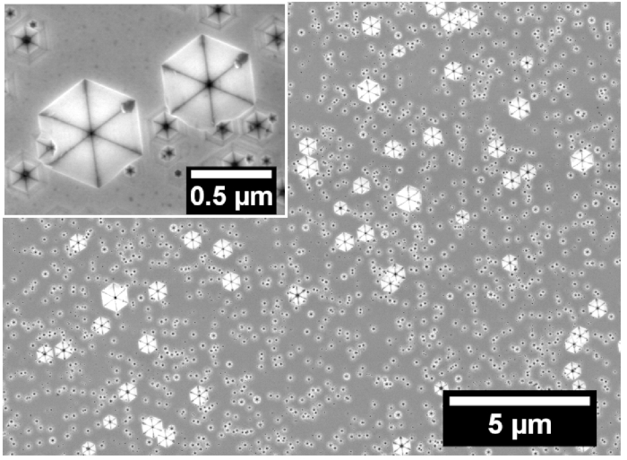
Figure 1: SEM micrographs of etch pits revealed on GaN surface using E+M etch. The etching parameters were set at 450 oC for 3 min.The inset depicts a magnified micrograph with revealed hexagonal pits generated on dislocation cores. The two biggest pits (>500 nm) represent dislocations with screw component of the Burgers vector. This figure has been reproduced with permission12. Please click here to view a larger version of this figure.
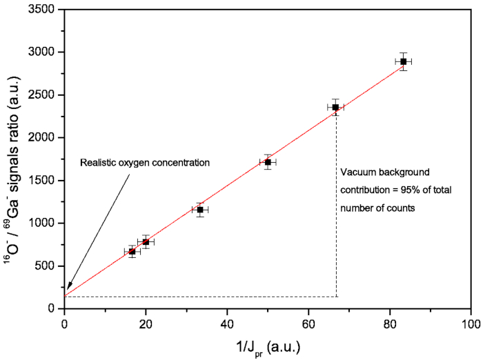
Figure 2: Average O- concentration vs. inverse primary current. Vacuum background contribution can be estimated from the plot. Error bars represent the standard deviation of each data set (five measurements). Please click here to view a larger version of this figure.
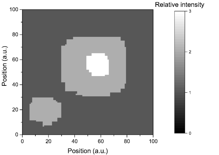
Figure 3: A typical 30Si2- secondary ion image for a blank silicon wafer. Intensity differences are caused by nonuniformity of the detector. Please click here to view a larger version of this figure.

Figure 4: Typical plane view of oxygen counts distribution measured in 3D mode. Shown are images (A) from raw data, (B) after flat-field correction, and (C) after subtraction of vacuum background contribution. This figure has been adapted with permission12. Please click here to view a larger version of this figure.
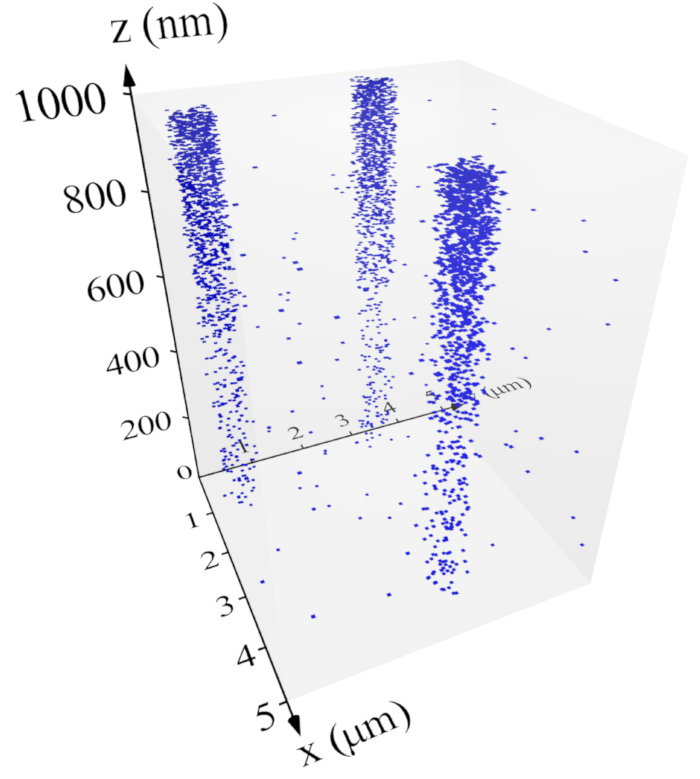
Figure 5: 3D view of oxygen counts in a 5 µm x 5 µm x 1 µm cuboid. For better visibility, the z-scale is elongated. See Supplemental Figure 1 for animation. This figure has been adapted with permission12. Please click here to view a larger version of this figure.
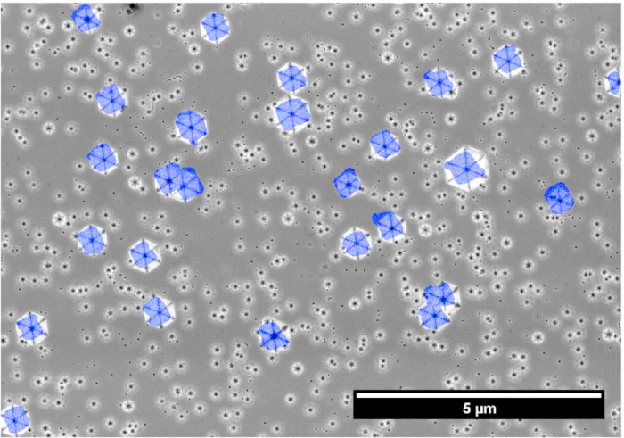
Figure 6: Lateral distribution of oxygen secondary ions (blue pixels) projected on SEM micrograph. Despite SIMS-related artifacts (lateral resolution determined by size of the primary beam), a clear correlation between the positions of largest pits and oxygen are observed. This figure has been adapted with permission12. Please click here to view a larger version of this figure.
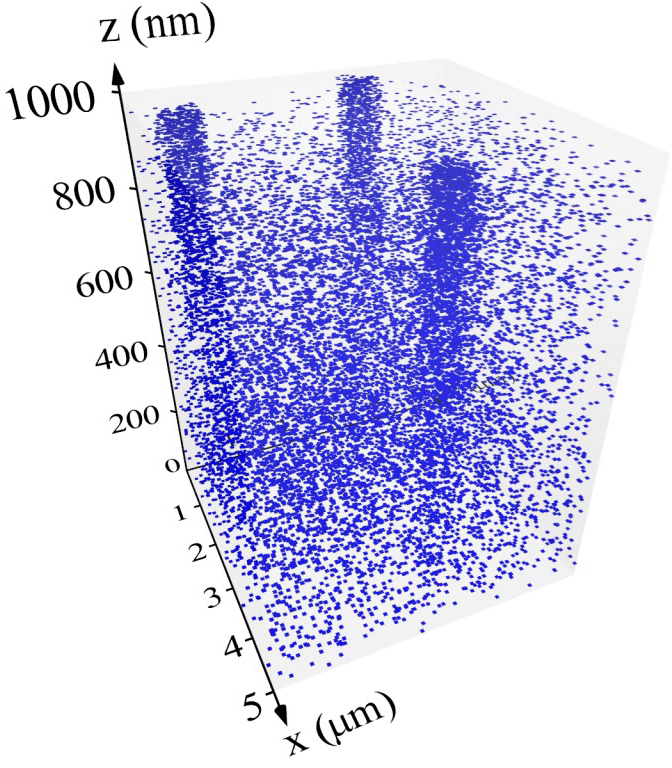
Figure 7: Animation showing how the reduction procedure is performed. At the beginning of the procedure, all counts are present, then for each layer, 90% of counts are randomly eliminated. Please click here to download this animation.
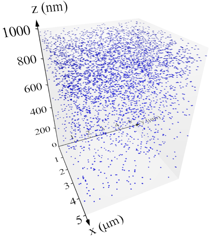
Figure 8: Random distribution of oxygen counts in suboptimal experiment. Please click here to view a larger version of this figure.
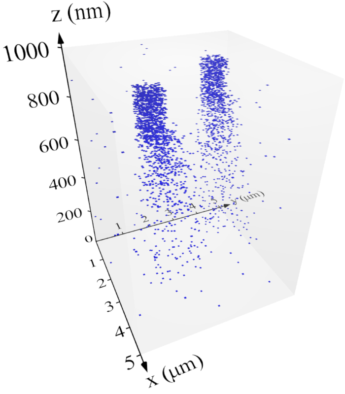
Figure 9: Experiment performed with an unstable beam. The quality deceases with sputtering depth. Please click here to view a larger version of this figure.
Supplemental Figure 1. Please click here to download this figure.
Discussion
Issues of nonuniformity of the detector and vacuum background contribution are easy to solve by flat-field correction and subtraction of parasitic counts, respectively. The subtraction procedure is not perfect, as it may subtract a contribution where oxygen has been agglomerated. In contrast, at the other position, it will leave the background count unaffected; thus, some artificial counts may still be present while some real counts are reduced. Nevertheless, it is efficient and sensitive enough to provide acceptable results.
The primary beam instability is the most problematic, as deterioration of the primary beam parameters will blur the secondary ion image; thus, no reliable information about the sample can be obtained. Section 3.2 in the protocol is particularly important. For instance, for a well-aligned beam, the first 30Si2- secondary ion image reflects nonuniformity of the detector, but after some time, the image will start to change. This is caused by deterioration of primary beam parameters (i.e., primary current loss, defocusing, position drift, etc.). It is therefore important to estimate the timespan of beam stability. It is advised to start the experiment 2-3 h after initialization of the beam, as it is typically more stable.
If the experiment is performed within a stable timespan of the beam and the result is still not satisfactory, it is advised to consider the quality of the primary beam. For a small primary beam, it is more challenging to confirm sufficient quality by observing a secondary ion image only. It is therefore advised to perform atomic force microscopy roughness tests at the crater bottom after sputtering ~1 µm of a very flat material (i.e., a blank silicon wafer). If the root mean squared roughness is above 1 nm, then further optimization of the primary beam is required.
The size of the beam limits the lateral resolution of this method. SIMS can image features that are smaller than the beam size, but the secondary ion image will inherit the shape and size of the primary ion beam. If a distance between two features is smaller than the size of the beam, the secondary ion image will blur them together. Despite these issues, the method allows users to obtain a realistic 3D distribution of impurities/dopants in solid state samples. Furthermore, any spatial segregation of atoms can be correlated to the position of defects and interfaces.
For GaN-based structures (i.e., oxygen-decorated), dislocations acting as local nonradiative recombination centers are responsible for n-type conductivity. For other materials any inhomogeneity of the dopant/contaminating atoms distribution may have major impacts on the performance of a device. Thus, the protocol is particularly useful for failure analysis and optimization of growth and processing procedures.
Disclosures
The authors have nothing to disclose.
Acknowledgements
This work was partially supported by the National Science Centre (NCN) within SONATA14 2018/31/D/ST5/00399 and OPUS10 2015/19/B/ST7/02163 projects.
Materials
| Name | Company | Catalog Number | Comments |
| Heating plate with ceramic top plate | IKA - Werke GmbH | 3644200 | for defect selective etching; yellow MAG HP 7 |
| Hydrochloric acid (HCl) solution 35-38% | Chempur | 115752837 | for etchant removal; pure p.a.; CAS: 7647-01-0 |
| Magnesium oxide (MgO) | Chempur | 116140200 | for eutectic solid etchant prepration; pure p.a.; CAS: 1309-48-4 |
| Potassium hydroxide (KOH) | POCH S.A. | 746800113 | for eutectic solid etchant prepration; pure p.a.; CAS: 1310-58-3 |
| Sodium hydroxide (NaOH) | POCH S.A. | 810925112 | for eutectic solid etchant prepration; pure p.a.; CAS: 1310-73-2 |
| Secondary ion mass spectrometer | CAMECA | IMS SC Ultra | |
| Scanning electron microscope | Hitachi | SU8230 |
References
- Wittmaack, K. High-sensitivity depth profiling of arsenic and phosphorus in silicon by means of SIMS. Applied Physics Letters. 29, 552 (1976).
- Ber, B. Y., et al. Secondary ion mass spectroscopy investigations of magnesium and carbon doped gallium nitride films grown by molecular beam epitaxy. Semiconductor Science and Technology. 13, 71-74 (1998).
- Chiou, C. Y., Wang, C. C., Ling, Y. C., Chiang, C. I. Secondary ion mass spectrometry analysis of In-doped p-type GaN films. Applied Surface Science. 203-204, 482-485 (2003).
- Emziane, M., Durose, K., Halliday, D. P., Bosio, A., Romeo, N. In situ oxygen incorporation and related issues in CdTe/CdS photovoltaic devices. Journal of Applied Physics. 100, 013513 (2006).
- Matsunaga, T., Yoshikawa, S., Tsukamoto, K. Secondary ion yields of C, Si, Ge and Cs surface density and concentration in SIMS. Surface Science. 515, 390-402 (2002).
- Gnaser, H. SIMS detection in the 1012 atoms cm−3 range. Surface and Interface Analysis. 25, 737-740 (1997).
- Peres, P., Merkulov, A., Choi, S. Y., Desse, F., Schuhmacher, M. Characterization of LED materials using dynamic SIMS. Surface and Interface Analysis. 45, 437-440 (2013).
- Arslan, I., Browning, N. D. Role of Oxygen at Screw Dislocations in GaN. Physical Review Letters. 91, 165501 (2003).
- Hawkridge, M. E., Cherns, D. Oxygen segregation to dislocations in GaN. Applied Physics Letters. 87, 221903 (2005).
- Arslan, I., Bleloch, A., Stach, E. A., Ogut, S., Browning, N. D. Using EELS to observe composition and electronic structure variations at dislocation cores in GaN. Philosophical Magazine. 86, 4727-4746 (2006).
- Hautakangas, S., et al. Gallium and nitrogen vacancies in GaN: Impurity decoration effects. Physica B: Condensed Matter. 376-377, 424-427 (2006).
- Michałowski, P. P., Złotnik, S., Rudziński, M. Three dimensional localization of unintentional oxygen impurities in gallium nitride. Chemical Communications. 55, 11539 (2019).
- Kamler, G., Weyher, J. L., Grzegory, I., Jezierska, E., Wosiński, T. Defect-selective etching of GaN in a modified molten bases system. Journal of Crystal Growth. 246, 21-24 (2002).
- Zhuang, D., Edgar, J. H., Strojek, B., Chaudhuri, J., Rek, Z. Defect-selective etching of bulk AlN single crystals in molten KOH/NaOH eutectic alloy. Journal of Crystal Growth. 262, 89-94 (2004).
- . . SC-Ultra, User's Guide. , (2005).
- Weyher, J. v. L., et al. Orthodox etching of HVPE-grown GaN. Journal of Crystal Growth. 305, 384-392 (2007).
Reprints and Permissions
Request permission to reuse the text or figures of this JoVE article
Request PermissionExplore More Articles
This article has been published
Video Coming Soon
Copyright © 2025 MyJoVE Corporation. All rights reserved